In the research and development of intelligent control, power electronics, and other fields, Hardware-in-the-Loop (HIL) simulation has become a core technology for shortening development cycles and reducing testing costs. Our independently developed HL1000 semi-physical simulation platform is equipped with 65 commonly used circuit topology models, meeting the needs of users in scientific research, teaching, or industrial testing.
01
Hardware Introduction

Hardware-in-the-Loop
Hardware-in-the-Loop simulation involves running simulation models on real-time processors to simulate the operating state of the controlled object, connecting to the test object through I/O interfaces.HIL simulation, also known as semi-physical simulation, integrates the hardware of the part of the system that needs to be simulated directly into the simulation loop. This not only compensates for many deficiencies in pure digital simulation, enhancing the confidence in the entire model, but also significantly reduces the programming workload. Another advantage of this simulation is that it enables real-time data interaction between the simulation model and the actual system, making the verification process of simulation results very intuitive and greatly shortening the product development cycle. During simulation, the computer is connected to the actual hardware through various information channels, and both the computer and the actual hardware work together to complete the simulation, analyzing the simulation results on the computer to assess the hardware’s operational status.The semi-physical simulation experimental platform independently developed by our company consists of the HIL_CONTROL control board and the HL1000 hardware-in-the-loop system, as shown in the figure below: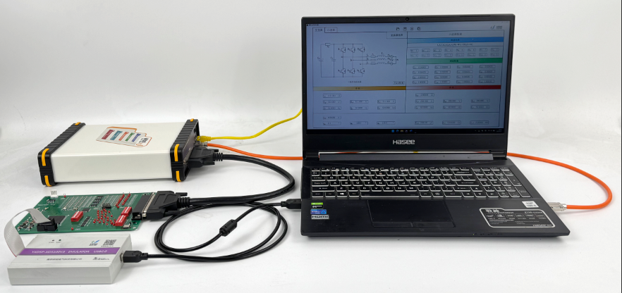
01
Introduction to HL1000
Our independently developed HL1000 semi-physical simulation platform is equipped with 65 commonly used circuit topology models, meeting the needs of users in scientific research, teaching, or industrial testing.
02
HIL_CONTROL Control Board
HIL_CONTROL is a controller developed by our company based on the TMS320F28377D chip, used in conjunction with HL1000 for online simulation of semi-physical models.The HIL_CONTROL control board comes pre-programmed with control software in the TMS320F28377D chip, which reads voltage, current, and other parameters from HL1000 according to the program, calculates the corresponding PWM control signals, and finally inputs the control signals into the circuit model of HL1000 to ensure the normal operation of the model.The HIL_CONTROL control board is equipped with test points for sampling signals and control signals, allowing real-time monitoring of sampling signals and control signals using oscilloscopes and other third-party testing tools.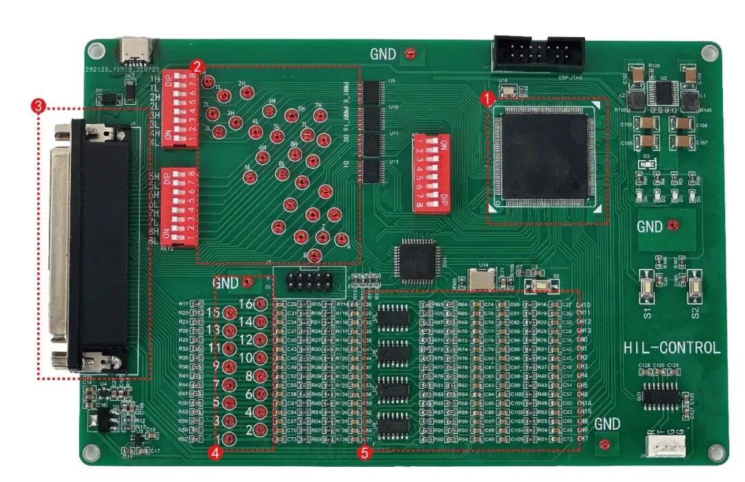
①: TMS320F28377D chip;
②: PWM control waveform measurement point;
③: DB62 socket;
④: Sampling signal measurement point;
⑤: Sampling signal conditioning circuit.

02
Connection Instructions

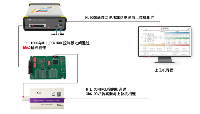 HL1000 needs to be connected to a network cable and a USB power supply cable, while the HIL_CONTROL control board needs to be connected to the XDS100V3 emulator. HL1000 and HIL_CONTROL control board are connected via DB62 ribbon cable, with power supplied to the HIL_CONTROL control board from HL1000 through the ribbon cable.HL1000 connects to the host computer via a network cable, enabling model operation and real-time data monitoring. The HIL_CONTROL control board connects to the host computer via the XDS100V3 emulator, allowing online debugging of the program through CCS.
03
Operating Environment Introduction

HL1000 Operating Environment
To use HL1000, the accompanying simulation software “YanXuHIL” must be installed on the host computer; simply extract the software installation package to use it. The software is shown in the figure below:
Figure 4_YanXuHIL Software
When the software is opened, it automatically loads the last opened model file.
HL1000 Software Icon
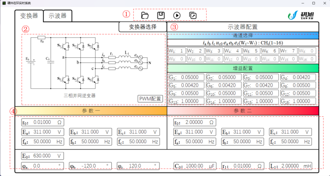
①: Function buttons;
②: Converter model circuit topology;
③: Channel selection and gain configuration;
④: Converter model hardware parameter settings.
Function Buttons
Function buttons include ID settings, saving model files, opening model files, and starting simulation buttons.
Circuit Topology
By clicking on the converter selection, different converter models can be selected, mainly includingDC-DC converters, AC-DC converters, motor control, new energy grid-connected power converters, and thyristor converters five categories.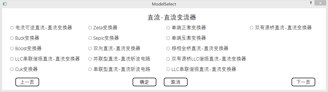
| DC-DC Converters | |
| Serial Number | Converter Type |
| 1 |
Bidirectional DC-DC converter |
| 2 | Buck converter |
| 3 | Boost converter |
| 4 | Buck-Boost converter |
| 5 | Cuk converter |
| 6 | Zeta converter |
| 7 | Sepic converter |
| 8 | Bidirectional DC-DC chopper circuit |
| 9 | Series DC-DC chopper circuit |
| 10 | Single-ended forward converter |
| 11 | Single-ended flyback converter |
| 12 | Phase-shifted full-bridge DC-DC converter |
|
14 |
Dual active bridge LLC resonant DC-DC converter |
| 15 | LLC series resonant DC-DC converter |
| 16 | Dual active bridge DC-DC converter |
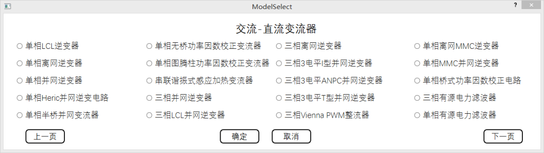
| AC-DC Converters | |
| Serial Number | Converter Type |
| 1 |
Single-phase LCL inverter |
| 2 | Single-phase off-grid inverter |
| 3 | Single-phase grid-connected inverter |
| 4 | Single-phase Heric grid-connected circuit |
| 5 | Single-phase half-bridge grid-connected converter |
| 6 | Single-phase bridge power factor correction converter |
| 7 | Single-phase totem pole power factor correction converter |
| 8 | Series resonant induction heating converter |
| 9 | Three-phase grid-connected inverter |
| 10 | Three-phase LCL grid-connected inverter |
| 11 | Three-phase off-grid inverter |
| 12 | Three-phase 3-level I-type grid-connected inverter |
| 13 | Three-phase 3-level ANPC grid-connected inverter |
| 14 | Three-phase 3-level T-type grid-connected inverter |
|
15 |
Three-phase Vienna PWM rectifier |
| 16 | Single-phase off-grid MMC inverter |
| 17 | Single-phase MMC grid-connected inverter |
| 18 | Single-phase bridge power factor correction circuit |
| 19 | Three-phase active power filter |
| 20 | Single-phase active power filter |
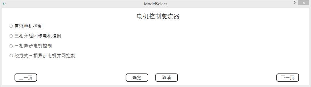
| Motor Control Converters | |
| 1 |
DC motor control |
| 2 | Three-phase permanent magnet synchronous motor control |
| 3 | Three-phase asynchronous motor control |
| 4 | Wound three-phase asynchronous motor grid control |
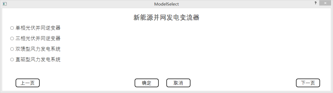
| New Energy Grid-connected Power Converters | |
| 1 |
Single-phase photovoltaic grid-connected inverter |
| 2 | Three-phase photovoltaic grid-connected inverter |
| 3 | Doubly-fed wind power generation system |
| 4 | Direct-drive wind power generation system |
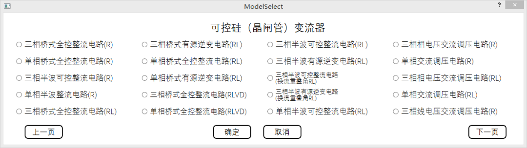
| Thyristor Converters | |
| Serial Number | Converter Type |
| 1 |
Three-phase bridge full-controlled rectifier circuit (R) |
| 2 | Single-phase bridge full-controlled rectifier circuit (R) |
| 3 | Three-phase half-wave controlled rectifier circuit (R) |
| 4 | Single-phase half-wave rectifier circuit (R) |
| 5 | Three-phase bridge full-controlled rectifier circuit (RL) |
| 6 | Three-phase bridge active inverter circuit (RL) |
| 7 | Single-phase bridge full-controlled rectifier circuit (RL) |
| 8 | Single-phase bridge active inverter circuit (RL) |
| 9 | Three-phase bridge full-controlled rectifier circuit (RLVD) |
| 10 | Single-phase bridge full-controlled rectifier circuit (RLVD) |
| 11 | Three-phase half-wave controlled rectifier circuit (RL) |
| 12 | Three-phase half-wave active inverter circuit (RL) |
| 13 | Three-phase half-wave controlled rectifier circuit (commutation overlap angle RL) |
| 14 | Three-phase half-wave active inverter circuit (commutation overlap angle RL) |
|
15 |
Single-phase half-wave controlled rectifier circuit (RL) |
| 16 | Three-phase phase voltage AC voltage regulation circuit (R) |
| 17 | Single-phase AC voltage regulation circuit (R) |
| 18 | Three-phase phase voltage AC voltage regulation circuit (RL) |
| 19 | Single-phase AC voltage regulation circuit (RL) |
| 20 | Three-phase line voltage AC voltage regulation circuit (R) |
| 21 | Three-phase line voltage AC voltage regulation circuit (RL) |
Channel Op-Amp Gain Ratio Explanation
The sampling channel selection part and PWM control part of HIL are fixed and cannot be changed, with a total of 16 PWM channels and 16 sampling channels, corresponding as labeled.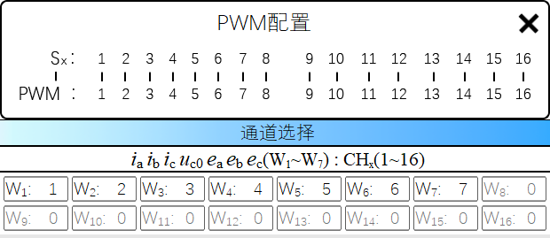
Figure_Channel Correspondence
The sampling gain configuration corresponds one-to-one with the sampling channels. The gain configuration part needs to consider that the output upper and lower limits of HIL are ±5V, and the voltage and current sampling part multiplied by the gain should not exceed 5V. For example, if the current gain is set to 20 times, the setting value is 1/20=0.05, and for the voltage gain of 240 times, the setting value is 1/240=0.0042.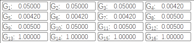
Figure_Sampling Channel Gain
Circuit Parameter Settings
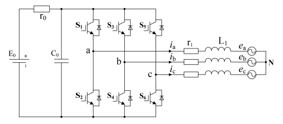
When setting circuit parameters, they can be compared with the circuit topology. Taking the three-phase grid-connected inverter as an example:
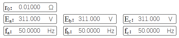
Figure_Parameter Settings
r0: DC power supply internal resistance, generally very small; too large will affect power supply output;
Ea/Eb/Ec: Peak value of three-phase AC phase voltage, default is 311V (phase voltage AC220V)
fa/fb/fc: Three-phase AC grid frequency, default is 50Hz;
E0: DC input of three-phase grid-connected inverter;
ψa/b/c: Phase of three-phase grid, with a phase difference of 120° between the three phases;
C0: DC side capacitance, stabilizing the DC input voltage;
r1: AC measurement line impedance;
L1: AC measurement filter capacitor, smoothing the AC voltage output of the inverter.
Parameter settings can be configured according to the actual circuit, and the “Open Model File” function button can be used to find example files for configuration.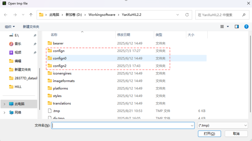
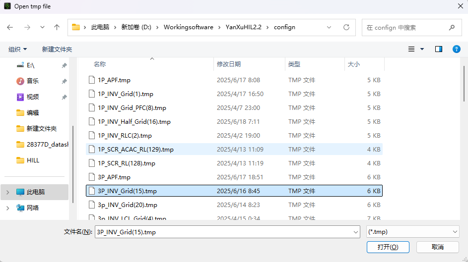
Figure_Example File
After completing the parameter configuration, click the function button “Start” to begin running the model. At this point, clicking on the oscilloscope allows real-time monitoring of the voltage and current data simulated by HIL1000.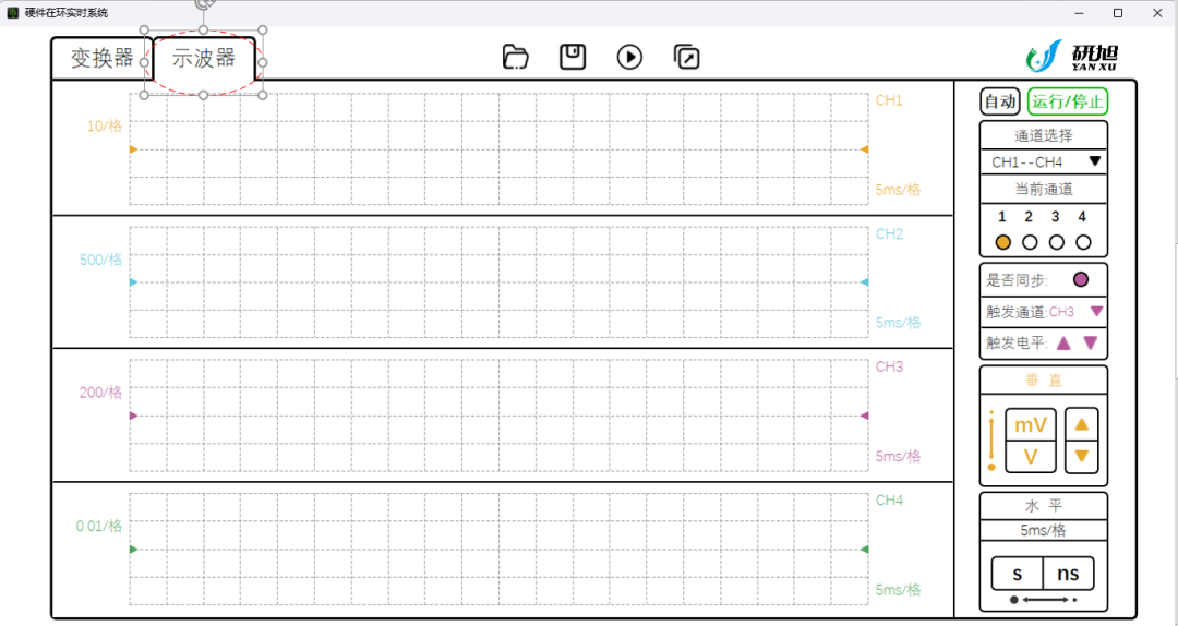
Figure_Oscilloscope Data Monitoring
HIL_CONTROL Control Board Operating Environment
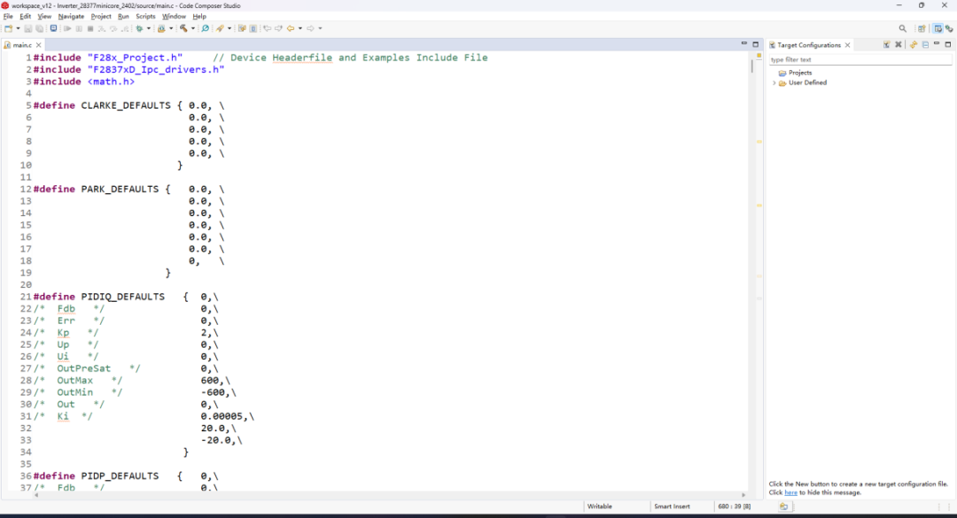
The HIL_CONTROL control board is designed based on the TMS320F28377D, and requires the use of Texas Instruments (TI) embedded system integrated development environment:Code Composer Studio (CCS), which can be used for software development for DSPs, microcontrollers, and application processors.
Figure_CCS Development Platform

04
Simulation Example

Taking the semi-physical simulation of a three-phase grid-connected inverter as an example
01
HIL_CONTROL Control Board Development
Open the CCS development platform and load the 28377 program for the three-phase grid-connected inverter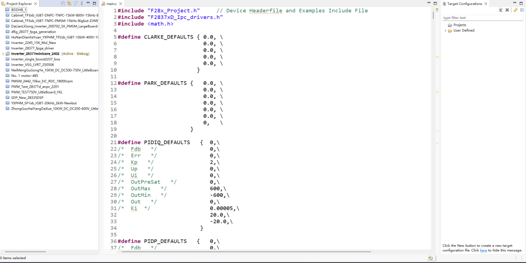
Figure_Three-phase Grid-connected Inverter 28377 Program
Configure Sampling Channels
For controlling the three-phase grid-connected inverter, it is necessary to collect three-phase voltage, three-phase current, and DC voltage, totaling 7 data points, thus requiring the first 7 sampling channels.Open the PCB schematic of the HIL_CONTROL control board, locate the sampling channel pins on DB62, and find the corresponding ADC sampling pins on the 28377D chip according to the electrical connections on the PCB schematic.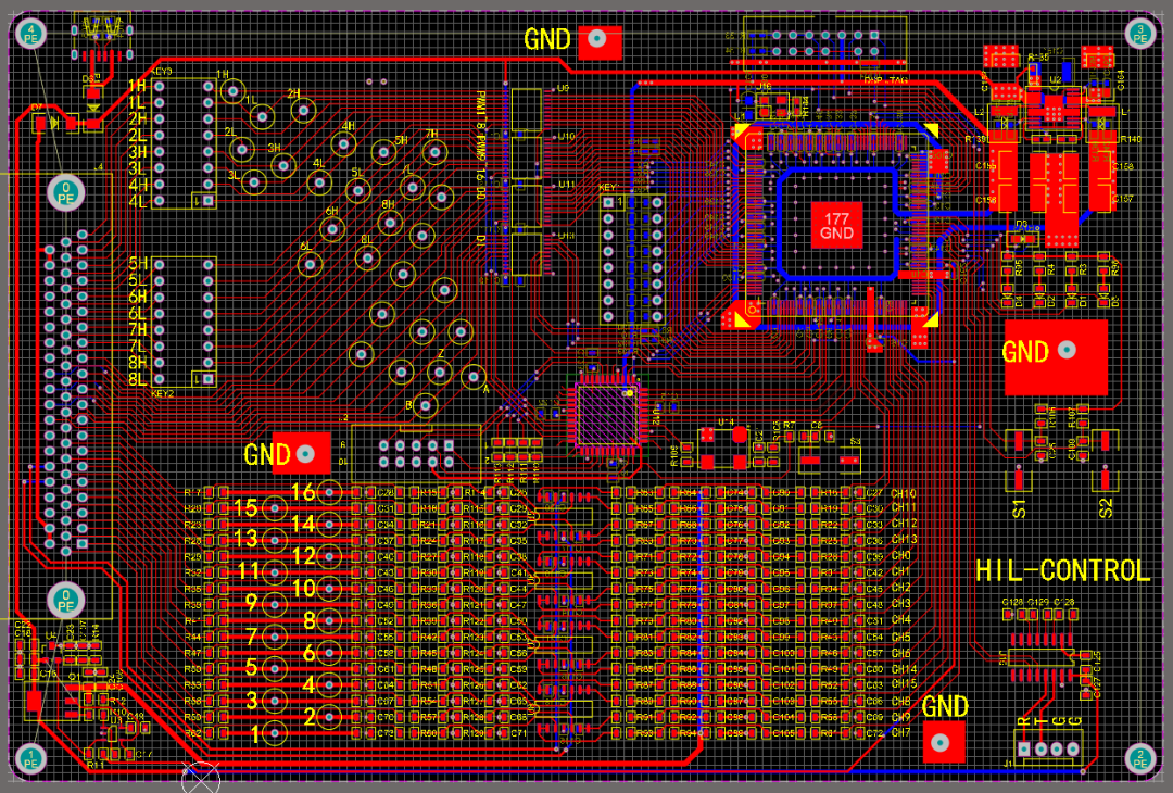
Figure_28377 Electrical Schematic
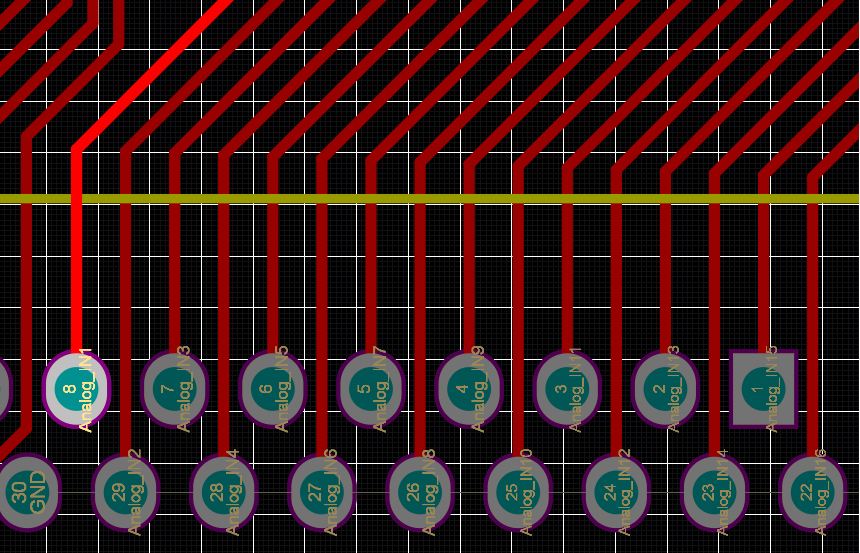
Figure_DB62 Sampling Channel Pins
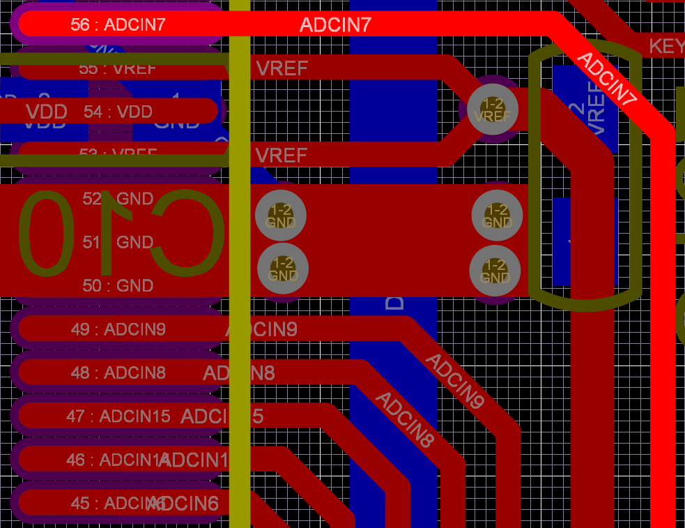
Figure_28377 Chip ADC Input Pins
After determining the correspondence between the ADC input pins of the 28377D chip and the DB62 sampling channel pins, configure the pins in the program according to the chip documentation.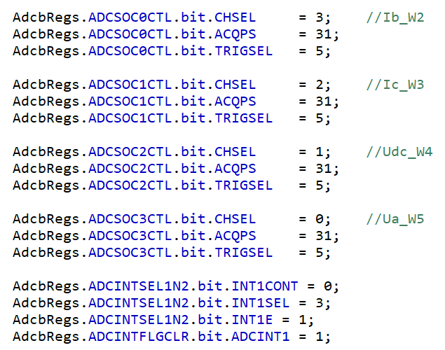
Figure_ADC Configuration
The 28377D chip sends the analog voltage and current signals collected from the ADC input pins to the analog-to-digital converter, converting them into digital values stored in the result register, and in the program, the value of the result register is assigned to a variable.
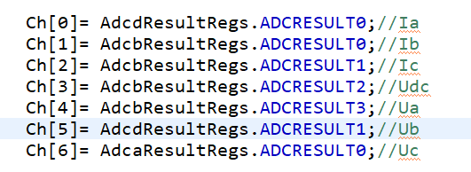
Figure_ADC Conversion Result Assignment
Then, according to the formula:
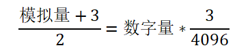
Where the analog value is the voltage value directly collected from the pin, its magnitude is the actual voltage and current parameters multiplied by the channel gain,thus obtaining
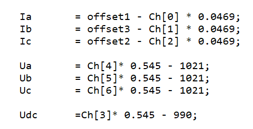
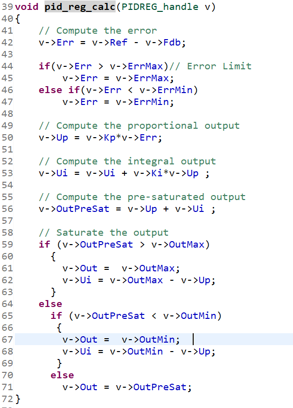
Figure_Actual Voltage/Current Sampling Values
Configure PWM Channels
This is consistent with the configuration of the sampling channels. First, find the correspondence between the DB62 socket pins and the chip pins, then configure the corresponding chip pins.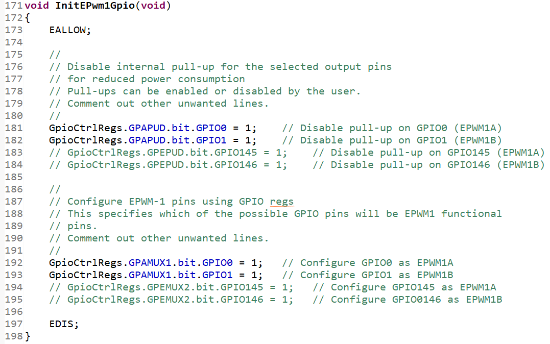
Figure_First Group PWM_GPIO Configuration
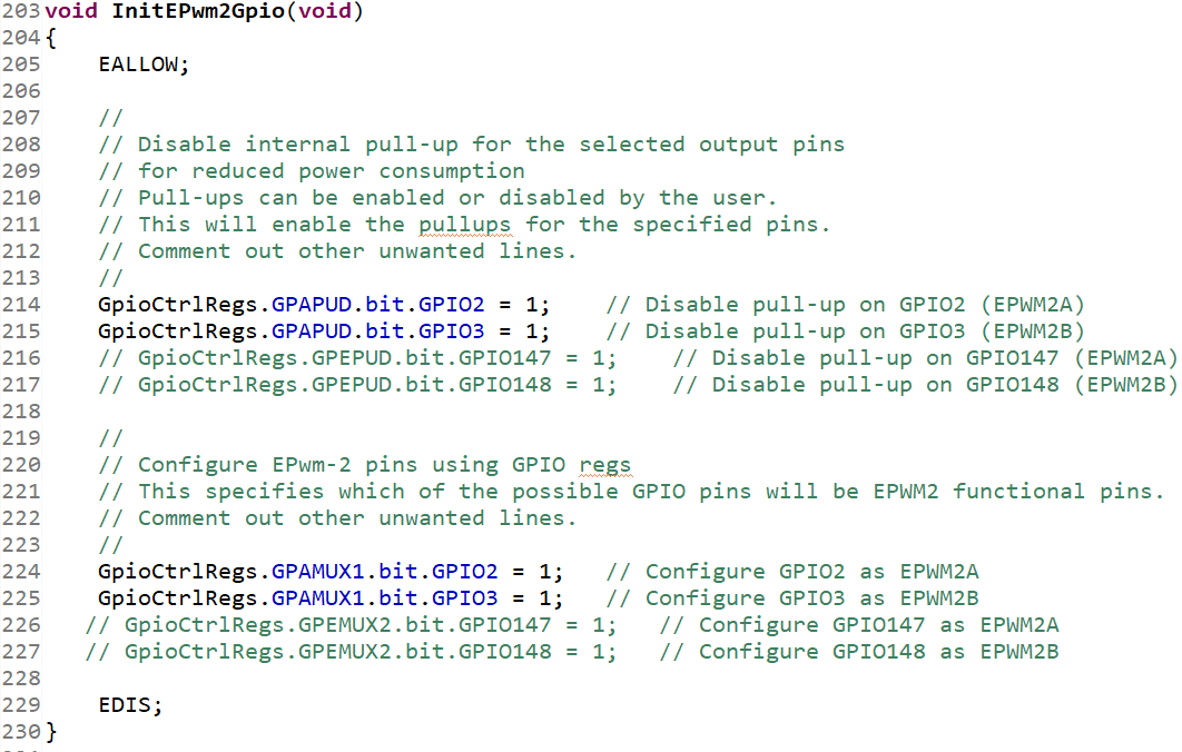
Figure_Second Group PWM_GPIO Configuration
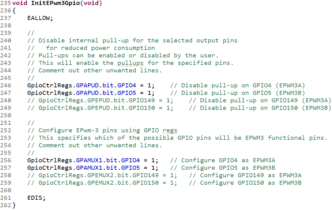
Figure_Third Group PWM_GPIO Configuration
Three groups of 6 PWM channels are used, with the chip GPIO corresponding one-to-one with the chip pins. The 6 PWM channels control the 6 switching devices of the three-phase full-bridge circuit.Adjusting PI ParametersAfter completing the configuration of the sampling channels and PWM channels, it is necessary to adjust the algorithm parameters in the program. The main adjustment method is to tune the PI parameters within the algorithm.First, perform Clarke and Park transformations on the sampled voltage/current parameters to convert them into the rotating coordinate system.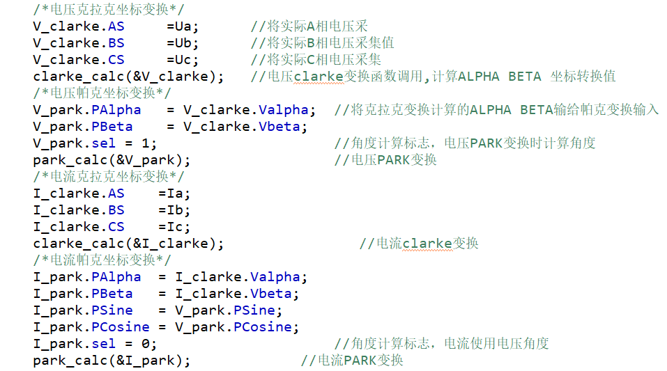
Figure_Clarke and Park Transformation
The output value of the voltage Park transformation is used as the input for the voltage outer loop, and the voltage setpoint is used as the reference for the voltage outer loop to calculate the error signal and perform PID calculations.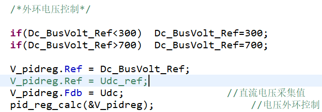
Figure_Voltage Outer Loop Calculation
The output value of the current Park transformation is used as the input for the current inner loop, and the result of the voltage outer loop calculation is used as the reference for the current inner loop to calculate the error signal and perform PID calculations.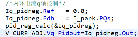
Figure_Current Inner Loop Calculation
Then, perform decoupling, inverse Park transformation, and other related calculations on the current inner loop calculation result to finally obtain the PWM duty cycle. The calculated duty cycle is loaded into the PWM output module of the chip to output the required PWM control waveform.
Throughout the process, we need to fine-tune the Kp and Ki of the PID calculations to stabilize the entire system’s operation.
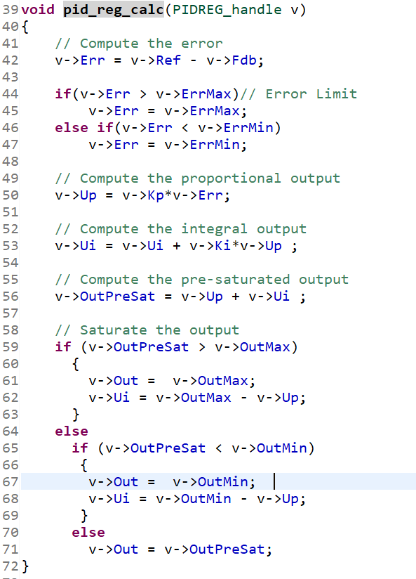
Figure_PID Calculation
Burn the modified program into the 28377D chip and perform online simulation. Monitor the program’s operation in real-time.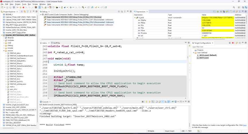
Figure_Program Online Simulation
HL1000 Online Simulation
Open the HL1000 simulation software and select the three-phase grid-connected inverter in the converter selection.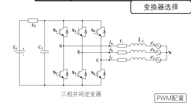
Figure_Converter Selection
Set the gain to a current gain of 20 times and a voltage gain of 240 times, i.e., G1/G2/G3 = 1/20 = 0.05, G4/G5/G6/G7 = 1/240 = 0.0042.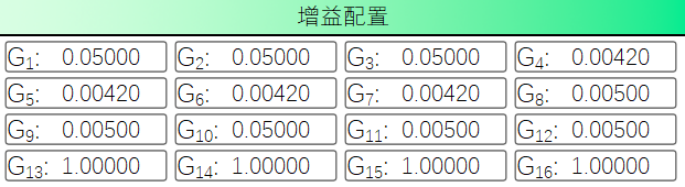
Figure_Gain Configuration
Set parameter one AC voltage phase peak value to 311V, frequency to 50Hz, and DC power supply internal resistance to 0.01Ω.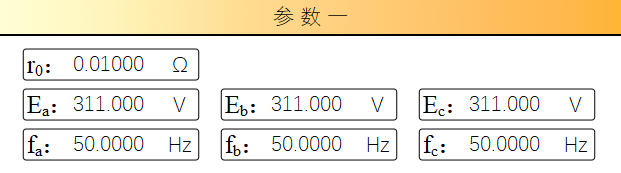
Figure_Parameter Setting 1
Set parameter two AC voltage phase peak value to 200V, frequency to 50Hz, and DC power supply internal resistance to 2Ω.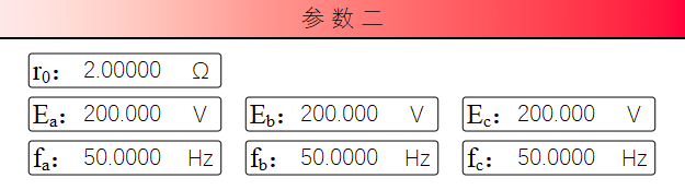 Set the DC voltage to 650V, with a phase difference of 120° between the three phases, DC capacitance of 1000uF, filter inductance of 2mH, and AC line impedance of 0.01Ω.

Figure_Parameter Setting 2
After completing the settings, click the start simulation button and enter the oscilloscope to monitor real-time current parameters.

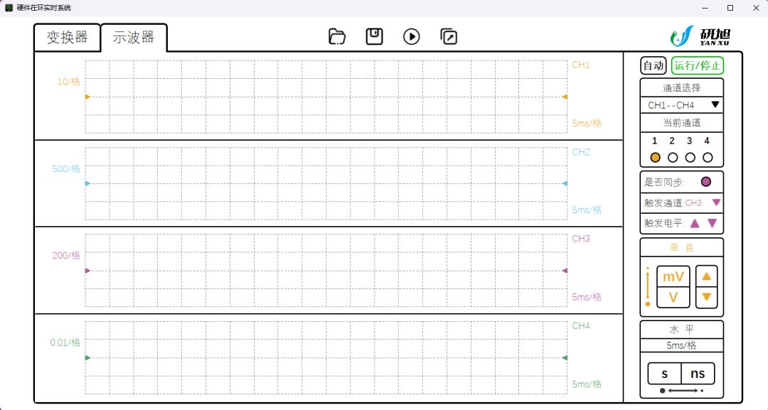
Figure_Running HIL1000

05
Display of Operating Results

CCS Software Simulation Results
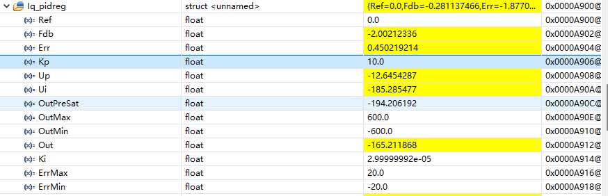
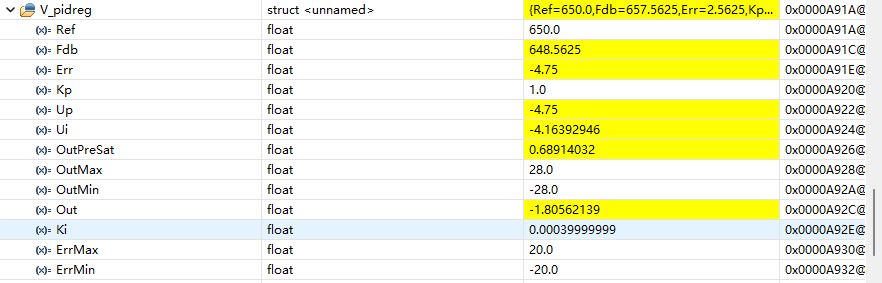
HL1000 Simulation Results
Simulation waveforms under different output currents.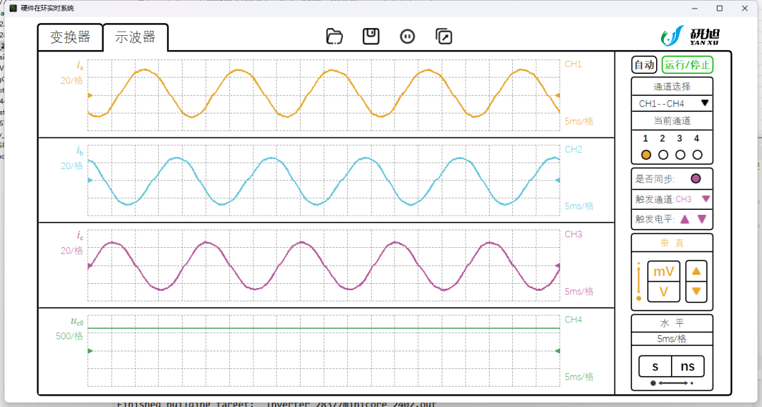
Figure_Grid-connected Current 20A
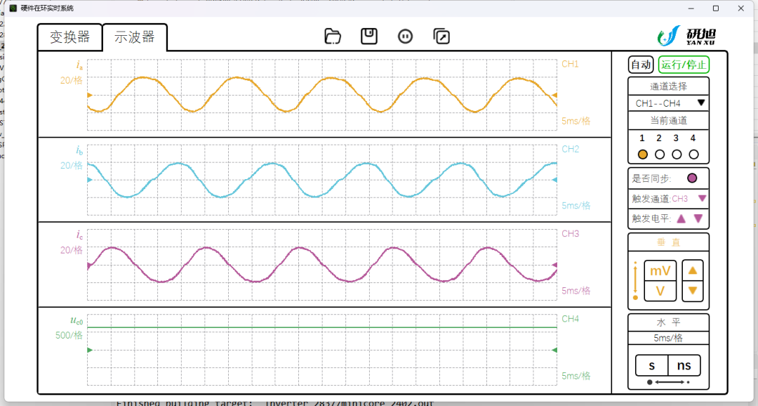
Figure_Grid-connected Current 14A
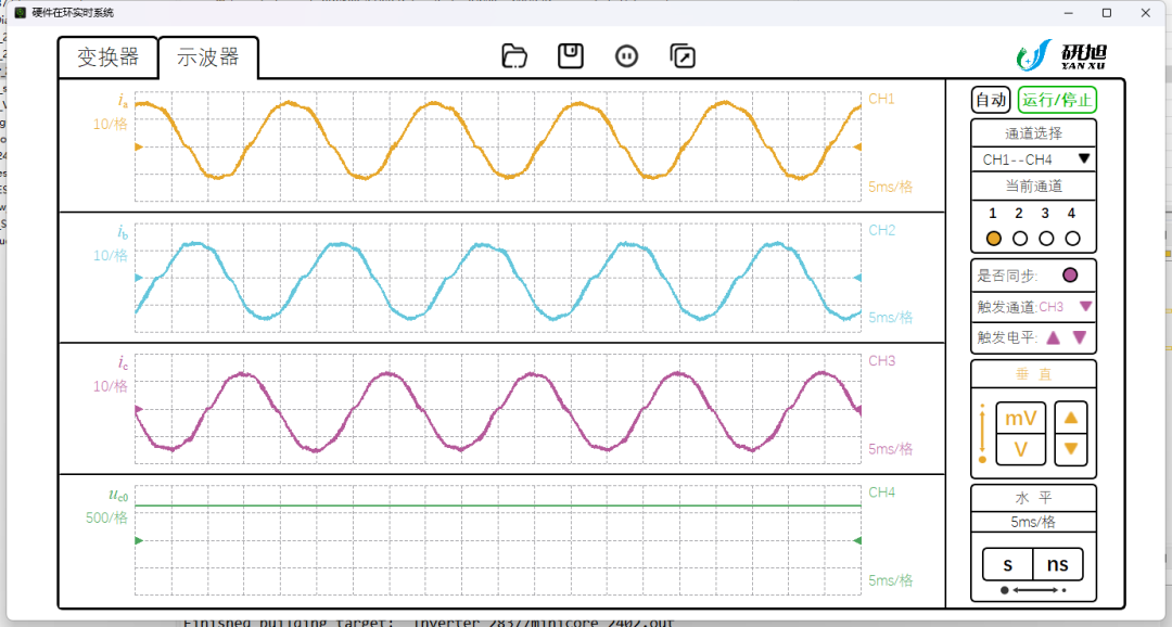
Figure_Grid-connected Current 10A
By clicking the parameter switch button on HIL1000, the circuit parameters can be switched from parameter 1 to parameter 2, achieving a grid step change.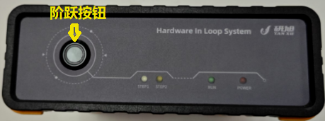 Demonstration of switching results: the amplitude of the AC voltage in parameter 2 is significantly reduced.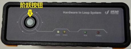
Figure_Parameter 1 AC Voltage Output
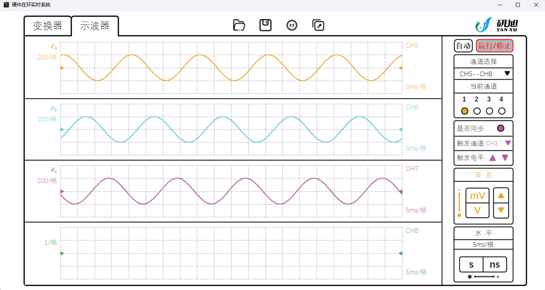
Figure_Parameter 2 AC Voltage Output
New Engineering Power Electronics and Motor Control Teaching Experiment Platform
YXMBD-TE1000