
Subtle Yet Unrecognized Low Power Design Techniques: Stack Effect
Continuing from the previous discussion:
We previously explained low power design techniques such as Clock Gating and Data Gating. Both can reduce the dynamic power consumption of circuits. The former can turn off the input clock signal of certain modules when they are idle, thereby reducing unnecessary clock transitions that cause dynamic power consumption. Similarly, the latter can fix the input of a computational module to a certain value when its computation results are not used (for example, when there is a MUX that is not selected), which avoids unnecessary computations and prevents signal transitions from propagating further. If the idle time is long enough, it can significantly reduce the dynamic power consumption of the circuit.
In fact, careful individuals might wonder what value is appropriate to fix the input to when using Data Gating. Is it arbitrary?
Of course, any input setting is possible, but different schemes will certainly vary. After employing Clock Gating and Data Gating, the module has no dynamic power consumption during idle time, so reducing static power consumption becomes an important goal. As process sizes shrink, static power consumption increasingly dominates, making it a critical area of research.
Low Power Design Technique: Stack Effect
So, what value should the input be set to in order to minimize the static power consumption of the circuit? This brings us to the Stack Effect.
Do you remember the previous post discussing how to reduce leakage power based on state-dependent information?
State-dependent Leakage Power
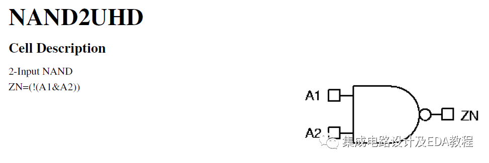
Two-input NAND gate:
Two-input NAND gate MOSFET circuit structure diagram:
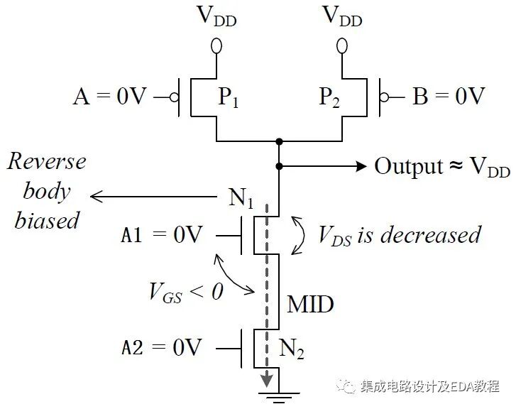
We mentioned that generally, when both inputs A1 and A2 are 0, the static leakage power is minimized. At this point, N1 and N2 are stacked together, and the potential between N1 and N2 is approximately Vdd/2. The Vsb of N1 is greater than 0, which raises its threshold compared to normal conditions, thus reducing leakage power. Additionally, the Vgs of N1 is less than 0, which further turns off the MOSFET, greatly reducing leakage.
This effect of having two MOSFETs with equal input potentials stacked on top of each other to reduce leakage power is referred to as the Stack Effect, which is quite effective in reducing circuit leakage power.
Summary of Stacked MOSFETs:
Some input patterns are significantly more effective than others in reducing Leakage Power;
1. Choose input patterns that minimize leakage power in combinational logic circuits;
We can use the stacked MOSFET method to reduce leakage power in combinational logic circuits during idle states.
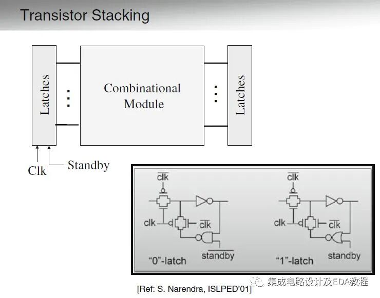
To effectively reduce leakage power, it is best to set specific input patterns for each combinational logic unit, but this is not very feasible as it would significantly increase control logic, potentially leading to counterproductive results. Therefore, it is more reasonable to select low power input patterns only for primary inputs.
As shown in the figure below, there are related articles that have published low power solutions using this technology: by adding a standby signal to the latch or register after a latch, it can control the combinational logic’s input to be set to 1 or 0 during idle states (whether to set it to 1 or 0 depends on which pattern has lower leakage power in standby).
2. Force one MOSFET to be split into two stacked MOSFETs;
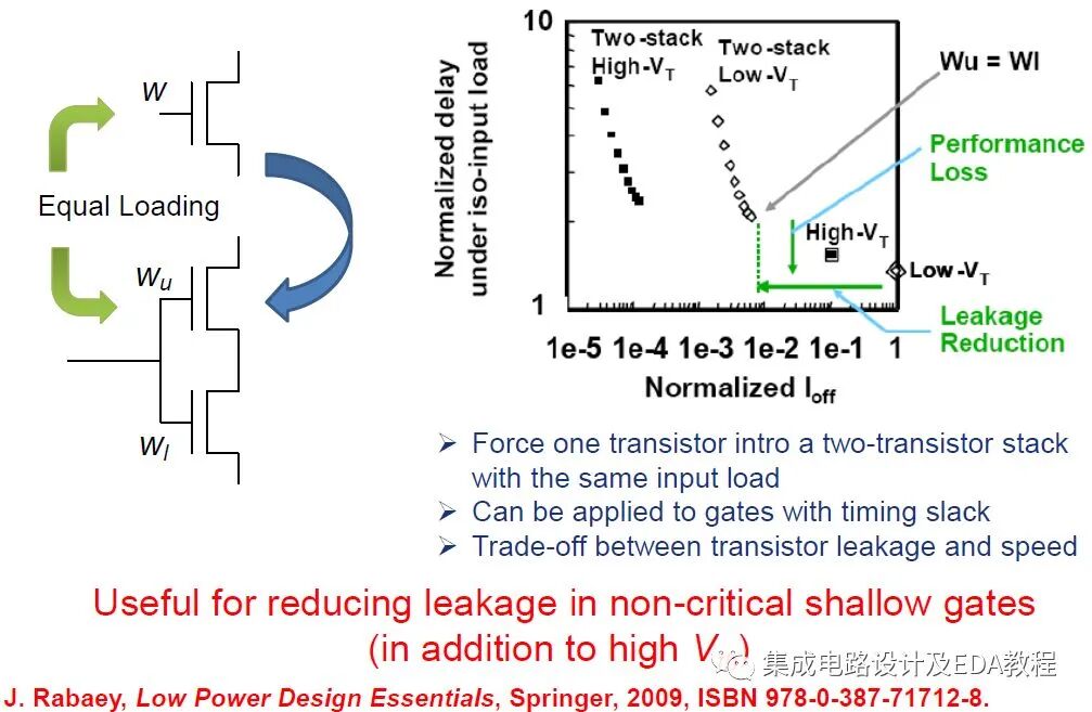
We can forcibly split one MOSFET into two stacked MOSFETs, both having the same input.
Note: This is actually a trade-off between leakage power and speed; it is best to apply this technique to units with timing slack, and it should not be used on timing-critical paths.
Effect: As seen in the figure, after using two-stacked MOSFETs, the leakage power of the Low-Vt MOSFETs in sleep mode is reduced by at least two orders of magnitude (from 1 to below 1e-2), while the leakage power of the High-Vt MOSFETs is reduced by at least three orders of magnitude (from 1e-1 to below 1e-4).
Summary of Stack Effect Low Power Technology:
Advantages:
Low cost, significant reduction in leakage power.
Disadvantages:
Effectiveness is limited; current EDA tools may not support it, requiring the development of CAD tools or using existing EDA tools to analyze and select appropriate input patterns.
This technology has played a role in our designs to some extent, though perhaps not intentionally. Just as we previously mentioned with the two-input NAND gate.
· END ·
*Disclaimer: Datong University maintains neutrality regarding all statements and views in original and reprinted articles. The articles are provided for readers’ learning and exchange. Copyright for articles, images, etc. belongs to the original authors. If there is any infringement, please contact us for removal!

2026 Autumn Recruitment Group



Mini Program Submission

☛ 2026 Autumn Recruitment Recommended Companies (Continuously Updated)
NVIDIA | Voda Semiconductor | STMicroelectronics | Weichuang Technology | Jingfeng Mingyuan | Juqian Technology | Aiwei Electronics | OmniVision Technologies | Xingchen Technology | Yanjing Microelectronics | Hengxuan Technology | Chipsea Technology | Guowei Electronics | Huada Electronics | Shengyu Technology | Gailun Electronics | NiuXin Semiconductor | Chip Alliance Technology | Mitralance | DeYi Microelectronics | Silicon Valley | Yuwei Semiconductor | KunNeng Semiconductor | Wayon | Zhuochen Technology | Ouyue Semiconductor | Silicon Semiconductor | Ankai Microelectronics | Zhongke Xinxin | ChaoWei Wujie
☛ Previous Articles Recommendations
[Autumn Recruitment] Beijing Venue Official Announcement! IC Industry Job Fair Registration Open →
Chengdu Venue Official Announcement! IC Industry Job Fair Registration Open →
IC Professionals, get ready! Xi’an Autumn Recruitment Job Fair is coming →
The 11th Shanghai Integrated Circuit Job Fair successfully concluded!
Average Salary of Listed Chip Companies in China Exposed!
30 Trillion Chip Companies Struggling to Survive?
These Chips Are Selling Like Hotcakes