Source: Content reprinted from WeChat public account “Yushi Capital”, thank you.
On September 13, 2020, Pacific Time, American graphics processing and artificial intelligence chip giant NVIDIA (NVDA US, no rating) announced on its official website plans to acquire the world’s largest processor core IP (Intellectual Property) supplier ARM Limited from Japan’s SoftBank and SoftBank Vision Fund for a total price of $40 billion in NVIDIA stock and cash. According to ARM’s official website, over 95% of smartphones globally are developed based on ARM IP. In the context of Sino-US trade friction, after the X86 architecture is firmly controlled by the United States, the ARM architecture may also be controlled by American companies, raising widespread market concerns about China’s lack of independent processor architecture and chip industry chain security.
Therefore, we conducted research and analysis on the history of processor development, ARM company, ARM’s cooperation with China, and the independent and controllable development of processor architecture. We believe that Chinese chip companies and ARM can achieve a win-win situation in cooperation during the mobile internet era, with domestic smartphones and multimedia SoC reaching world-leading levels, and high-end 32-bit MCUs achieving breakthroughs. The future era of smart IoT brings extremely rich application scenarios and demands for smart devices, and domestic MCUs and SoCs based on ARM architecture have broad development space. Meanwhile, we believe that NVIDIA’s acquisition of ARM may reshape the global chip industry landscape. Against the backdrop of Sino-US trade friction, the ARM architecture has the potential to become a regulated technology due to its technological and market position. We believe this uncertainty may stimulate the acceleration of China’s independent process. The RISC-V architecture, with its advantages of open-source and openness, is expected to become the best choice for China’s AIoT field’s independent and controllable processor architecture.
From thousands of transistors to tens of billions of transistors, CPU has developed rapidly in the past fifty years.
The Central Processing Unit (CPU) is the core of computer systems. The main functions of the CPU are to process instructions, execute operations, control timing, and process data. The CPU mainly includes components such as the logic unit, controller, and registers. At the same time, the CPU also includes a cache and the buses that connect data and control between them. Among them, the logic unit is a multifunctional arithmetic unit that mainly performs related logical operations, such as executing shift operations and logical operations. In addition, the logic unit can also perform fixed-point or floating-point arithmetic operations, as well as address calculations and conversions. The controller is mainly used to analyze instructions and can issue corresponding control signals. Registers are used to temporarily store instructions, data, and address information.
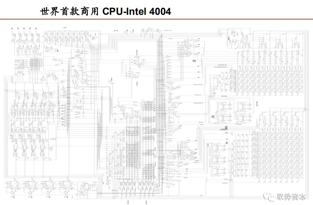
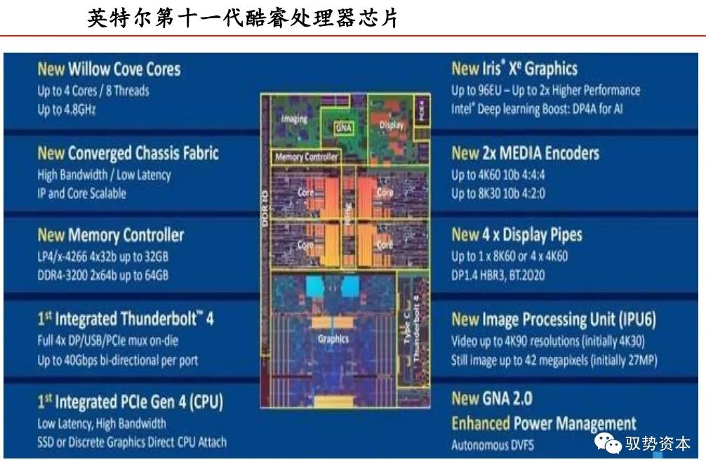
On November 15, 1971, American Intel Corporation (INTC US, no rating) launched the world’s first commercial computer microprocessor, the Intel 4004, which is considered the beginning of CPU development history. As a 4-bit processor, the Intel 4004 was built using a 10um process on a 2-inch wafer, integrating 2,300 transistors, with a main frequency of 740kHz. Fast forward 49 years to 2020, the 11th generation Core processor chip is based on Intel’s 10nm process, integrating over ten billion transistors, with a maximum frequency of up to 4.8GHz. This CPU chip is no longer a single CPU but integrates various components, including the newly architected Willow Cove core, Iris X graphics processor, memory controller, image processor, media decoder, power management, neural accelerator, and various high-speed interface controllers. Among them, the Willow Cove core is the traditionally defined CPU integrated into this CPU chip.
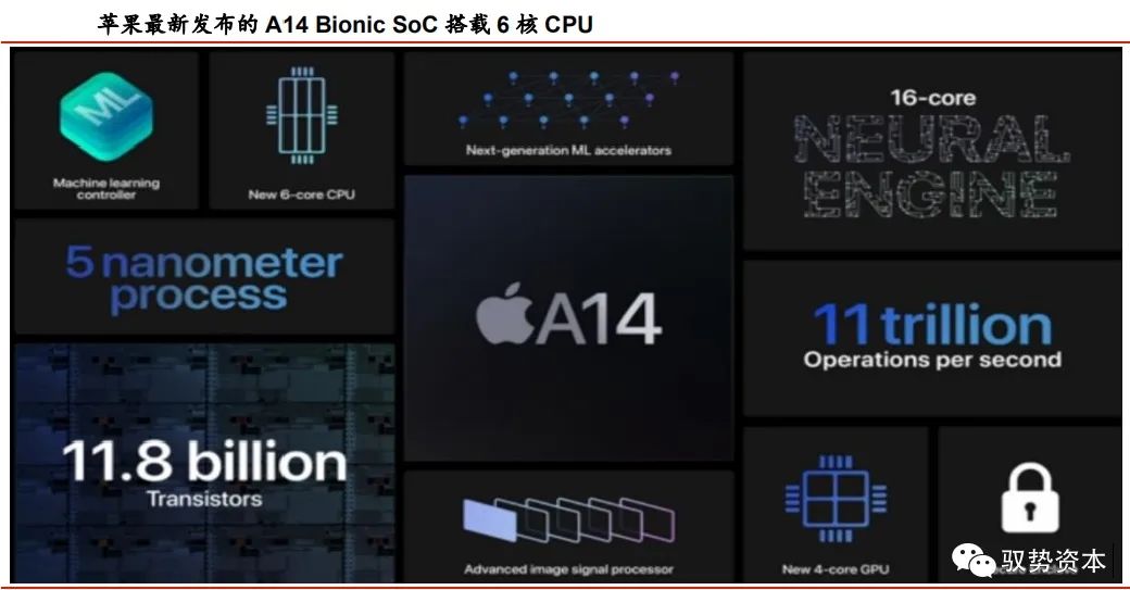
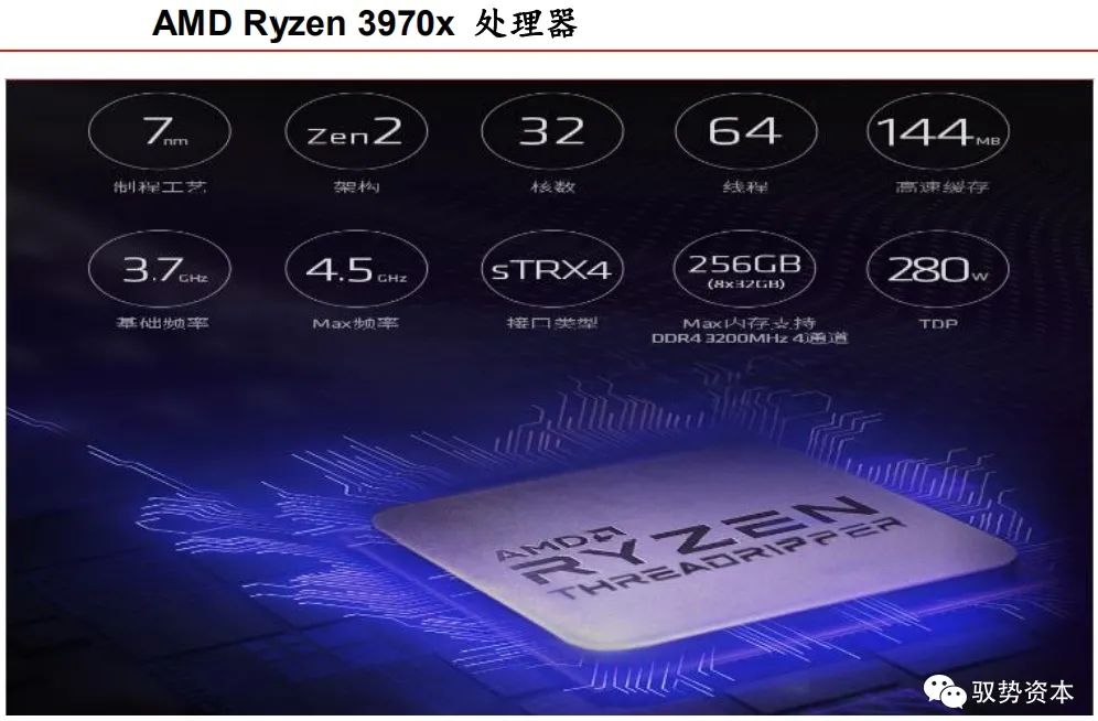
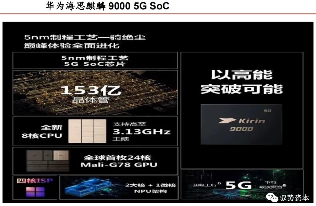
Modern CPUs have become one of the core components of processor chips, not just the sole component. Over the past 50 years, chip process technology has evolved from dozens of microns to 5 nanometers under the guidance of Moore’s Law, and the integration level of chips has continuously improved. Modern application processor chips (AP), microprocessors (MPU), microcontrollers (MCU), and system on chips (SoC) integrate various functional components around the CPU. These ultra-large-scale integrated circuit CPU modules are referred to as processor cores. The Apple 5nm mobile terminal processor chip A14 Bionic, released on October 14, 2020, integrates 11.8 billion transistors. On October 22, 2020, Huawei released the Kirin 9000 5G SoC, which integrates over 15 billion transistors.
The emergence of multi-core technology integrates multiple CPU cores on the chip substrate, further enhancing the performance of modern processor chips. Multiple cores are integrated into a CPU cluster that shares a level 1 cache. In 2012, ARM introduced big.LITTLE technology, integrating high-performance big cores (Cortex-A7x) and low-power small cores (Cortex-A5x) into the SoC’s CPU cluster, allowing switching between different application scenarios to balance performance and standby time. The big.LITTLE CPU cluster is most commonly seen in smartphone chips.
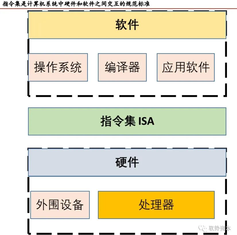
The instruction set architecture is the specification standard for CPU control and computation instructions.
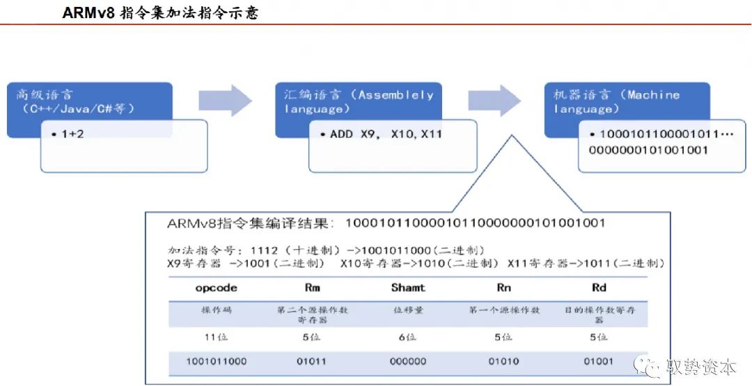
Computer instructions are commands that can be directly recognized by computer hardware. Instructions are composed of a string of binary codes. An instruction usually consists of two parts: the opcode and the address code. The opcode specifies the type or nature of the operation that the instruction is to perform, such as fetching data, performing addition, or outputting data; the address code specifies the content of the operation object or the address of the storage unit. A computer program is executed on hardware and is composed of thousands of instructions. A segment of a program is translated into assembly language through a compiler and then translated into machine code line by line by an assembler. These machine codes are represented by the machine language consisting of 0s and 1s, which are the computer instructions.
The instruction set architecture (ISA) refers to a set of instructions used to compute and control a computer system in a type of CPU. The instruction set architecture mainly defines instruction formats, addressing memory access (addressing range, addressing mode, addressing granularity, memory access method, address alignment, etc.), data types, and registers. The instruction set typically includes three major types of instructions: arithmetic instructions, branch instructions, and memory access instructions. Additionally, it includes architecture-related instructions, complex operation instructions, and other special-purpose instructions. Therefore, the instruction set architecture executed by a CPU not only determines the capabilities required by the CPU but also defines the instruction format and the structure of the CPU. The X86 architecture and ARMv8 architecture fall within the scope of instruction set architectures.
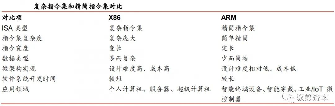
Instruction set architectures can be classified into two categories based on their complexity: Complex Instruction Set Computer (CISC) and Reduced Instruction Set Computer (RISC). CISC and RISC instruction set architectures emerged sequentially in the optimization development of computer instruction systems. In the early stages of computer development, the optimization direction of computers was to set some complex instructions that implement commonly used functions originally realized by software, using hardware instruction systems to improve the execution speed of the computer. Such computer systems are called complex instruction set computers. In the 1980s, the basic idea of simplifying computer instruction functions was proposed, retaining simple instructions that can be executed within a single clock cycle while implementing more complex functions via a subroutine. Such computer systems are called reduced instruction set computers.
The X86 architecture is currently the only mainstream complex instruction set that monopolizes the personal computer and server processor market. The X86 architecture was released by Intel in 1978. Over the past 40 years, the x86 family has continuously expanded, transitioning from desktops to laptops, servers, and supercomputers. Currently, the X86 architecture is controlled by three companies: Intel, Advanced Micro Devices (AMD US, no rating), and Taiwan’s VIA Technologies. Among them, Intel and AMD’s X86 processors dominate the desktop and laptop markets. According to a 2017 IDC report, X86 processors hold a market share of up to 96% in the server market. According to Mercury Research statistics, in 2019, VIA only held 0.1% of the X86 desktop processor market share.
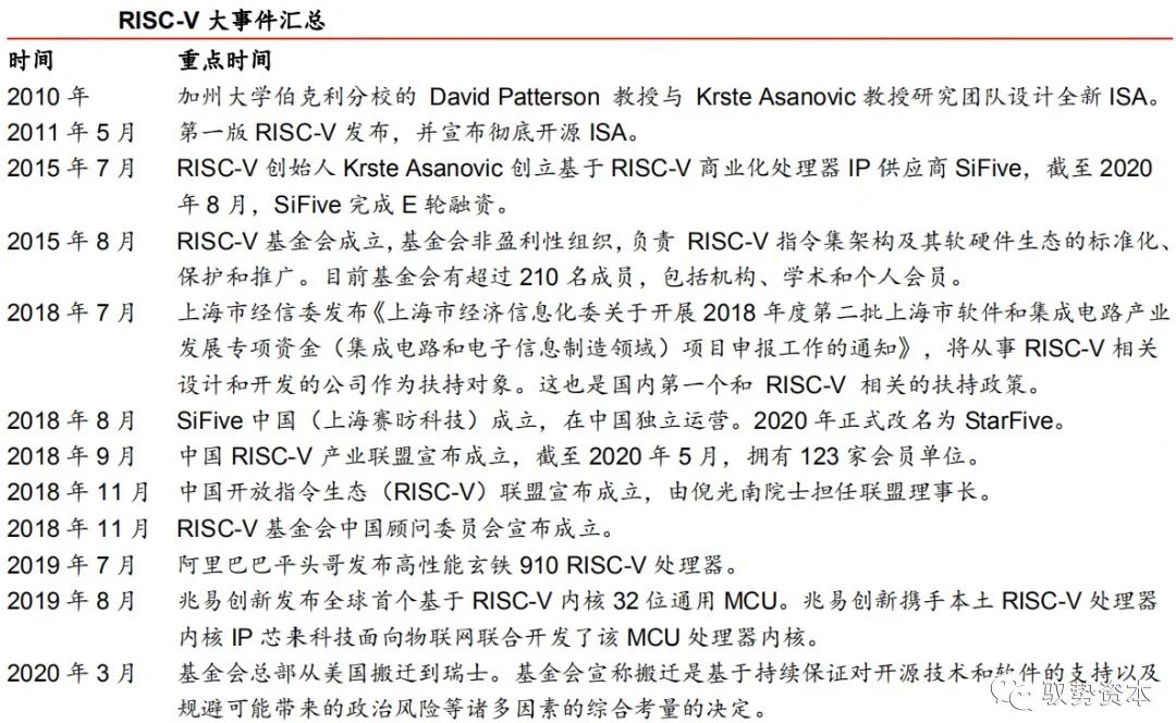
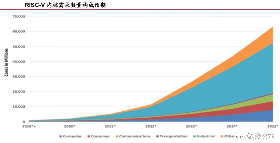
The ARM instruction set architecture, as the most successful RISC architecture, dominates the smartphone and IoT chip processor market. According to NVIDIA’s announcement, ARM-based chips have shipped a total of 180 billion units. ARM architecture processors account for over 90% of the market share in smartphone chips, automotive information chips, wearable devices, and IoT microcontrollers. In the 1990s, MIPS and Alpha, as well-known RISC architectures, failed in the competition with X86 in the computer market and missed the opportunity of rapid development in smart terminals. The RISC-V architecture, released in 2010, has attracted significant attention from academia and industry worldwide due to its open-source nature. Top global universities, research institutions, and chip giants have participated, and governments have introduced policies to support the development and commercialization of RISC-V.
Processor microarchitecture is the physical implementation of the instruction set architecture.
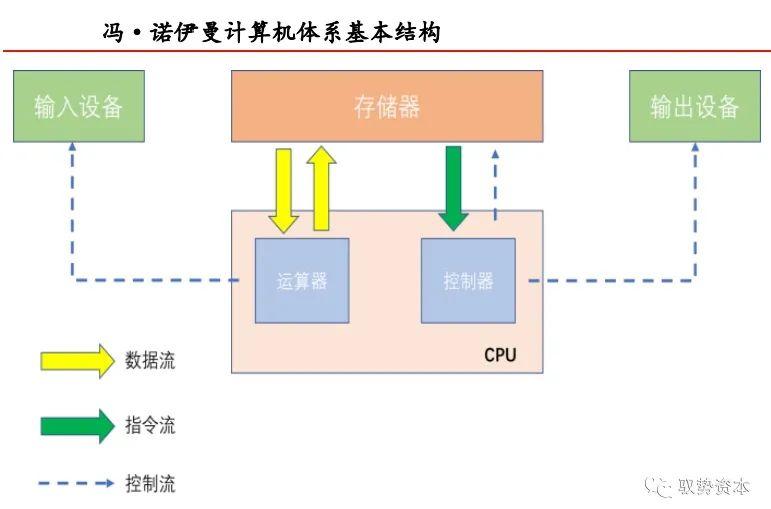
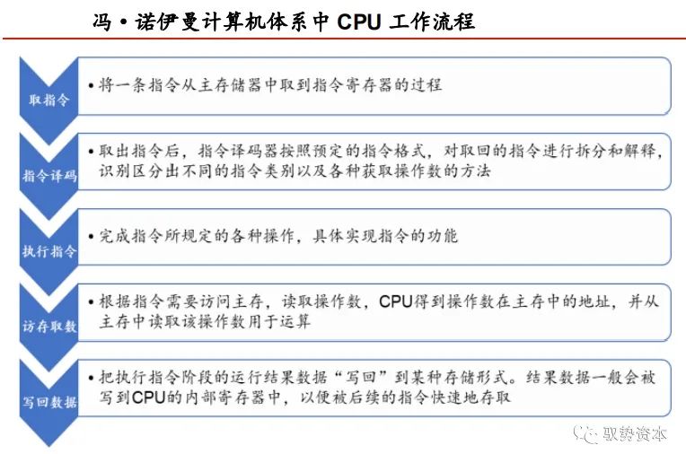
The von Neumann architecture is the foundation of modern computers. In 1946, Hungarian-American scientist John von Neumann proposed the stored-program concept, treating the program itself as data, storing the program and the data it processes in the same way, and defining the five main components and basic working methods of stored-program computers. The von Neumann architecture mainly consists of the CPU, memory, and input/output devices. Under this architecture, instructions and data need to be accessed from the same storage space and transmitted via the same bus, which cannot be executed concurrently. The CPU work in the von Neumann architecture is divided into five stages: instruction fetch, instruction decode, execute, read memory, and write back.
The Harvard architecture is another major computer architecture. Compared to von Neumann processors, the Harvard architecture has two independent memory modules for instructions and data, using two separate buses to connect the CPU and memory modules. In the modified Harvard architecture, instructions and data exist in two independent memory modules but share the address and data buses. In modern complex chips, pure von Neumann or Harvard architectures can be seen, but most often a combination or coexistence of both architectures is observed.
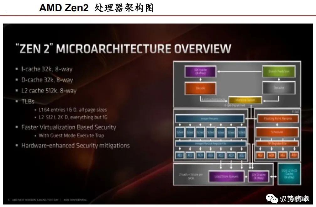
The physical circuits that implement the instruction set architecture are called the microarchitecture of the processor. In simpler terms, the processor architecture refers to the processor circuit. Generally, companies that possess the capability to independently design processor microarchitecture are considered to have processor R&D capabilities. In most cases, the microarchitecture of a processor is a physical implementation targeted at a specific instruction set architecture. A small number of processor architectures are designed for better compatibility and implement multiple instruction set architectures in their circuit design. Although instruction set architectures can be licensed to multiple companies, the design details of the microarchitecture, that is, the physical implementation of the instructions, are kept strictly confidential by each vendor. Due to different functional requirements of processors, usage scenarios, and differences in design technology among companies, even based on the same instruction set architecture, various companies will design and produce different processor architectures.
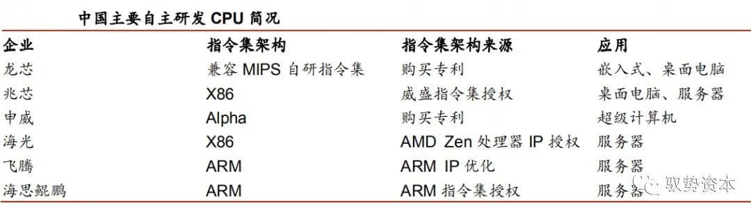
In the computer era, major processor manufacturers such as Intel and AMD develop processor architectures that only supply their own processor chips. As monopolists of personal computers and servers, the X86 architecture camp, Intel and AMD continue to maintain a model of designing processor cores solely for their own processor chips. In 2016, AMD collaborated with Chinese server company Haiguang, and the Zen architecture licensed to Haiguang is the processor microarchitecture. This licensed product is actually the processor circuit designed by AMD based on the X86 architecture, not the X86 instruction set architecture. Even such IP licensing cooperation is a rare example in the X86 camp.
In the nearly 20 years since the rise of smart mobile devices, the ARM model, represented by kernel microarchitecture IP licensing, has emerged. After developing kernel microarchitectures, ARM sells them as IP, allowing chip manufacturers to design chips based on ARM-licensed kernels for use or external sales. The ARM architecture-based kernel microarchitecture IP is diverse, designed to be concise and reliable, and performs excellently in low-power domains. This licensing model has achieved widespread success in mobile intelligent fields represented by mobile terminals such as smartphones and tablets, set-top boxes, video surveillance, and other application media chips. As a result, ARM has become the dominant processor IP licensor in the mobile internet era.
Industry division of labor has become more refined, and ARM has become the king of processor IP licensing.
The vertical division of the semiconductor industry has spawned the chip IP industry.
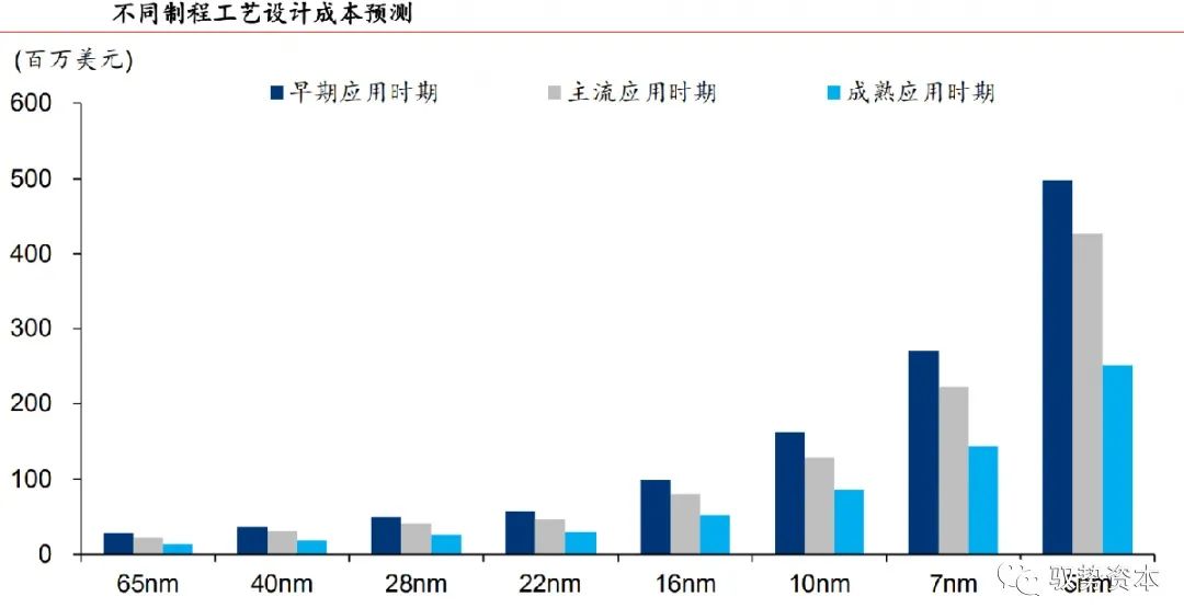
Starting in the 1990s, the core of the information industry transitioned from personal computers to mobile phone industries, moving from an internet-dominated phase to a mobile internet phase. Smart mobile terminals and smart multimedia products have become more complex and diverse, increasing the complexity of design due to differentiated chip functionality and performance requirements. On the other hand, as Moore’s Law progresses, the design and development resources and costs for advanced process chips continue to increase. According to a 2020 IBS report, the design cost of a first-generation chip using a 5nm process could reach $497 million, an increase of up to five times compared to 16nm; even if 5nm becomes a mature process in the future, the design cost of a single chip could still reach $250 million, nearly the design cost of a first-generation 7nm chip. Under the trend of fabless + foundry + OSAT (design without a fab + foundry + packaging testing), the global semiconductor industry continues to refine its division of labor, and the chip design industry has further split into the chip IP (Intellectual Property) industry.
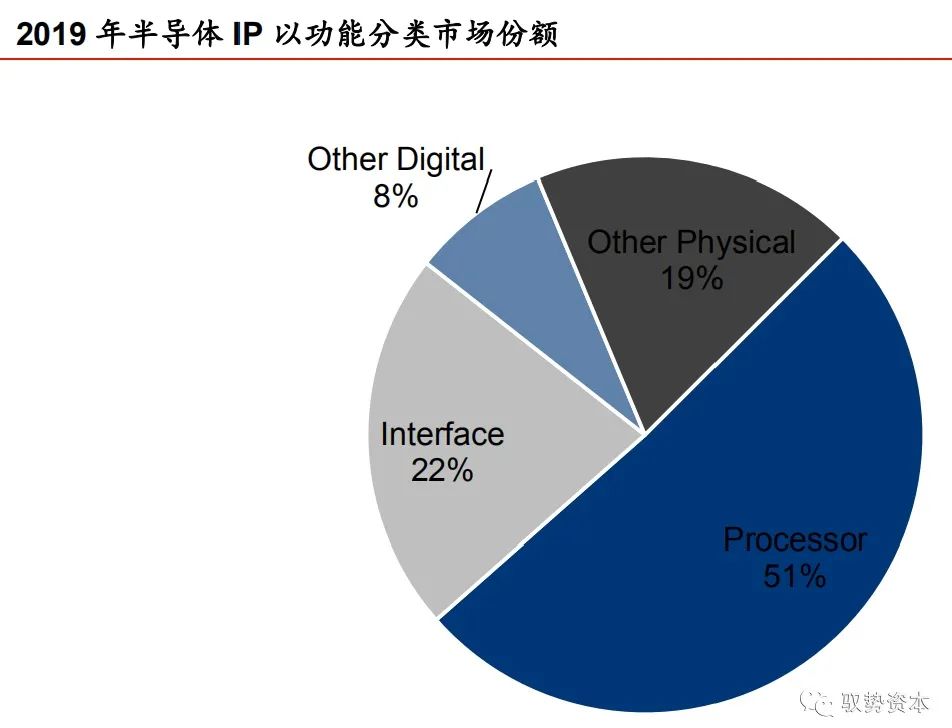
Semiconductor IP refers to validated, reusable integrated circuit modules with specific functions. IP suppliers focus on developing IP microarchitectures and profit by charging IP architecture licensing fees and royalties. Design companies can directly integrate licensed IP into their chips to achieve functionality without redeveloping it. According to Markets and Markets, the semiconductor IP market is expected to reach $6.5 billion by 2024, driven by the continuous advancement of multicore technology and the increasing demand in modern SoC design. Based on IP functionality segmentation, processor IP occupies the largest market share, with CPU, GPU, NPU, VPU, DSP, and ISP processor IP accounting for 51% of the entire market in 2019, according to IPnest statistics.
ARM and the mobile internet era have achieved mutual success.
ARM stands for Advanced RISC Machines, headquartered in Cambridge, UK. The company was established in November 1990 as a joint venture between Apple Computer, Acorn Computer Group, and VLSI Technology. ARM does not manufacture chips or sell actual chips to end customers but licenses its RISC ISA and processor design solutions for partners to produce distinctive chips. ARM’s architecture licensing model has enabled it to achieve a win-win situation with its partners, rapidly becoming the creator of the global standard for reduced instruction set microprocessors. On July 2016, Japan’s SoftBank announced a £24.3 billion acquisition of ARM, but the business remains independently operated.
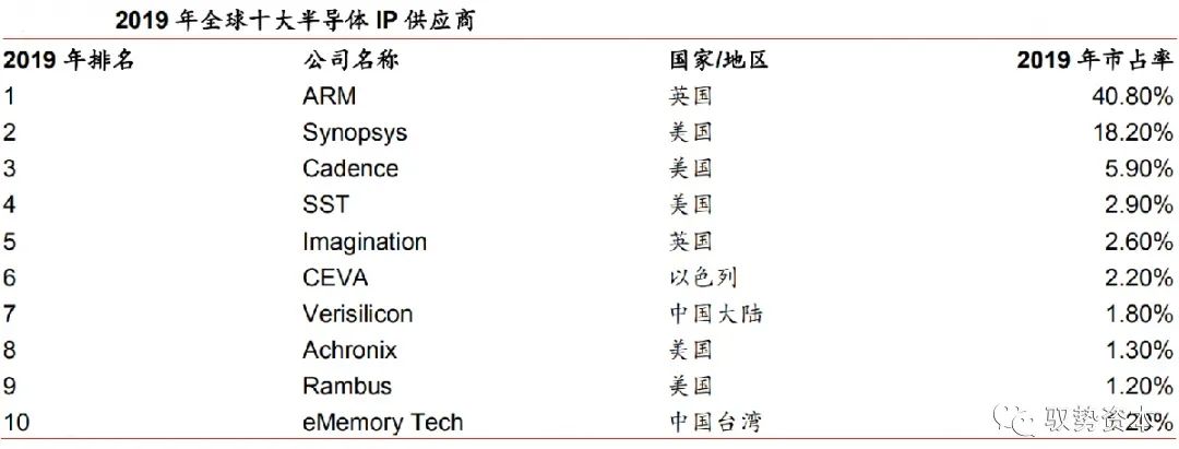
With its monopoly advantage in the general processor IP field, ARM ranks first among global IP suppliers in terms of IP revenue. ARM processor cores developed based on the ARM instruction set are widely used in smartphones, televisions, cars, smart homes, smart cities, and wearable devices. According to market share data released by SoftBank in 2017, over 99% of smartphones, modems, over 95% of automotive information devices, and over 90% of wearable devices are equipped with ARM architecture processors.
ARM does not sell chips but licenses architecture, pioneering a new business model in the semiconductor industry.
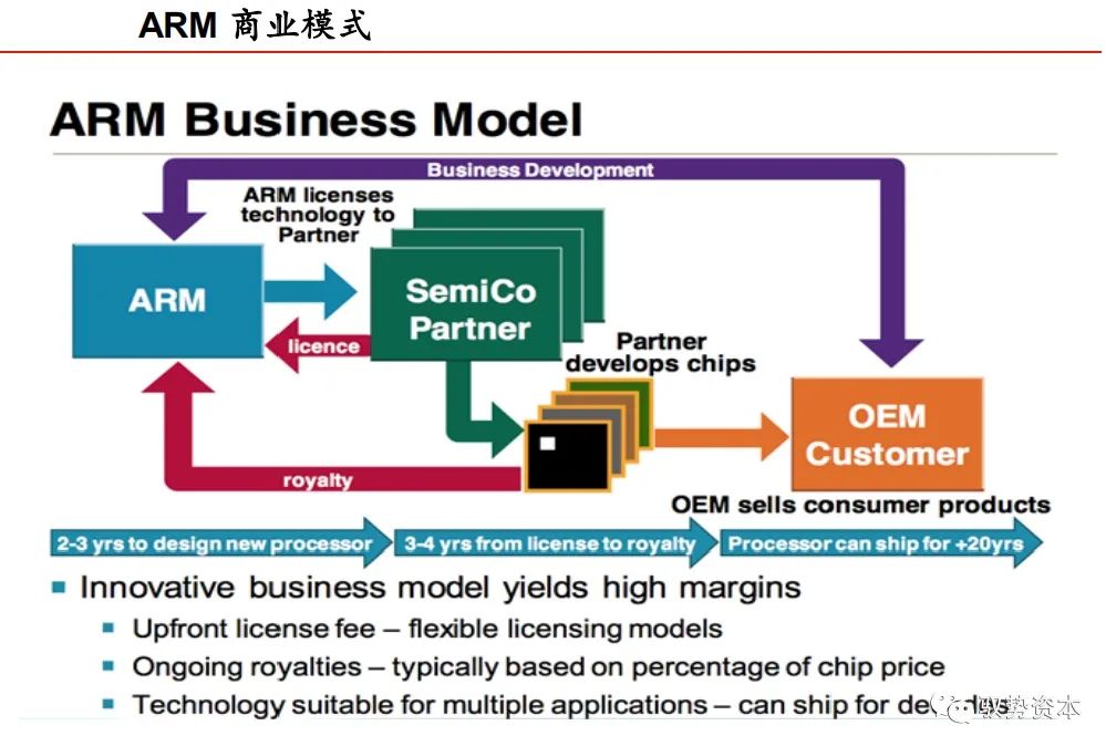
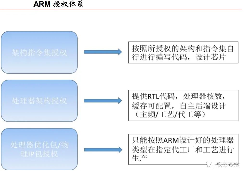
As a semiconductor company, ARM’s unique business model does not design and manufacture entire chips but focuses on licensing processor core architectures. ARM has consistently maintained a neutral position as a processor IP supplier. This neutral position has helped ARM widely promote the ecosystem based on its architecture through licensing. ARM’s processor architecture licensing is divided into two levels: one is ARM instruction set architecture licensing, and the other is ARM processor architecture licensing. The company’s revenue sources include: 1) licensing fees from semiconductor companies, which are one-time fees for a certain period; 2) royalty fees from semiconductor companies when they sell chips to other customers, where ARM earns a certain percentage of royalty income for each chip produced; 3) fees for providing technical consulting services to semiconductor companies and users.
ARM tightly integrates with its partners through instruction set architecture licensing.
ARM instruction set architecture licensing refers to ARM licensing its RISC reduced instruction set to the licensee. The licensee can make significant modifications to the ARM instruction set, even expanding or reducing it. Afterward, the licensee develops a processor architecture based on their modified instruction set, achieving differentiated design at the source of the processor architecture, maintaining control over their self-developed chips, achieving unique competitiveness while still being compatible with ARM’s complete ecosystem. In this cooperation model, ARM forms a highly close technological partnership with its partners.
Apple’s A-series processors are a successful example of self-developed cores based on ARM instruction set architecture licensing. In September 2012, Apple released the A6 processor SoC with the launch of the iPhone 5, marking the beginning of Apple’s self-developed processor cores based on ARM architecture. In September 2013, Apple was the first to release the dual-core A7 processor based on the ARMv8 architecture, which was the world’s first 64-bit smartphone processor, outperforming the competing Android camp’s 32-bit quad-core solutions. The A-series processor core’s performance has surpassed all competitors in the Android camp, and this trend continues to this day. In 2020, Apple claimed that the newly released A14 Bionic chip’s performance is comparable to some laptop processors.
Apple announced at WWDC 2020 that Mac computers will transition to using self-developed processors based on ARM architecture. We believe that Apple’s decision to end its 15-year partnership with Intel and switch to self-developed ARM processors aims to further close Apple’s hardware and software ecosystem. Apple hopes to achieve full autonomy in hardware, creating a competitive advantage similar to the success of the iPhone. From ARM’s perspective, if Apple succeeds, it will also help ARM realize its long-standing ambition to break the X86 monopoly in the personal computer market.
ARM provides diversified processor core IP licensing, achieving a win-win with ecosystem partners.
ARM processor architecture licensing refers to ARM licensing its self-designed processor core IP to customers. Customers can directly integrate the core RTL (Register Transition Level) code into the chip processor module during front-end chip design. Customers can also configure the processor’s cache, core count, and frequency. By connecting to other functional modules, peripheral interfaces, and main storage interface modules through the system bus, a complete chip is generated. ARM provides a variety of family processor IP solutions for various application scenarios, covering high-performance computing, high-performance real-time, low-power embedded, cloud computing, hardware security, and high-performance machine learning. ARM’s processor IP licensing model provides reliable processors while reducing chip development costs, promoting innovation in applications. The extensive partnerships enrich ARM’s ecosystem, establishing ARM’s dominant position in processor markets such as smartphones and IoT in the intelligent era.
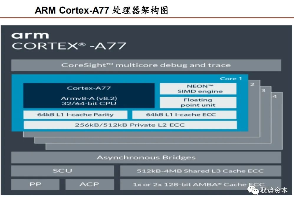
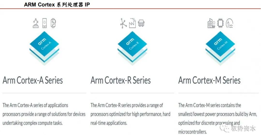
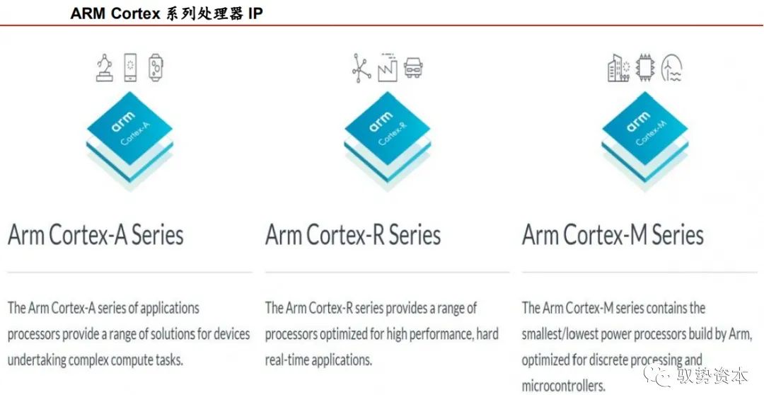
ARM Cortex series processor cores are the core series occupying the processor IP market. Among them, the Cortex-A series targets high-performance computing needs and applications running rich operating systems and program tasks, such as smartphones, tablets, set-top boxes, digital TVs, routers, and monitoring SoC chips. The Cortex-A series includes high-performance big core product lines represented by the A7x series and low-power small core product lines represented by the A5x series.
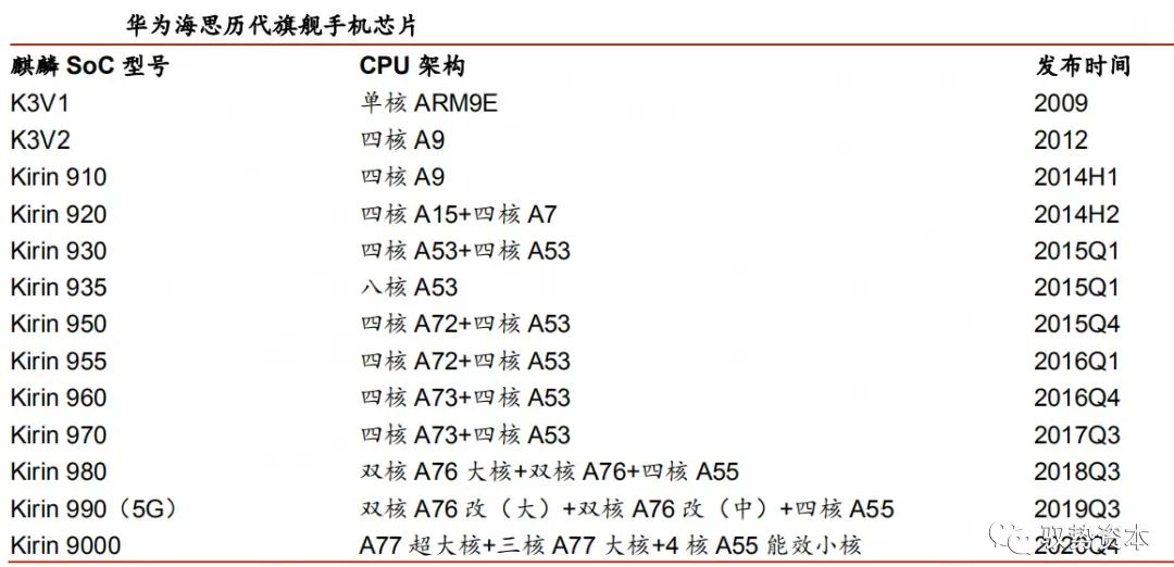
Modern multi-core SoCs often integrate a certain number of big and small cores to balance peak performance and low power consumption. Big cores handle short-term high-performance tasks, while small cores handle low-performance tasks or support background tasks during standby. Currently, except for Apple’s self-developed processor cores, Android smartphone SoC design companies, led by Qualcomm, HiSilicon, and MediaTek, use the Cortex-A7x and A5x combination as the core cluster configuration. Among them, Qualcomm and Huawei will make varying degrees of optimizations in architecture.
Compared to Cortex-A processor cores, Cortex-M processor cores are designed to be smaller in area and more energy-efficient. Typically, these processors have shorter pipelines, simpler designs, lower maximum clock frequencies, and excellent power performance. The Cortex-M series has a very broad application prospect in the current smart interconnected era, covering smart measurement, human-machine interface devices, automotive and industrial control systems, large household appliances, consumer products, and medical devices. Currently, Cortex-M occupies a dominant position in the global 32-bit MCU market. The Cortex-R processor series targets high-performance processors for real-time applications, operating at relatively high clock frequencies with very low response latency. They are mainly used in hard disk controllers, automotive transmission systems, and baseband control in wireless communications.
ARM helps domestic chips achieve both quality and quantity, and the acquisition may stimulate the acceleration of independent control.
With the proliferation of smart mobile devices, ARM Cortex-A supports the rise of domestic smart terminal SoC.
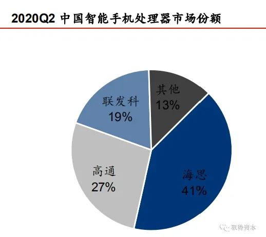
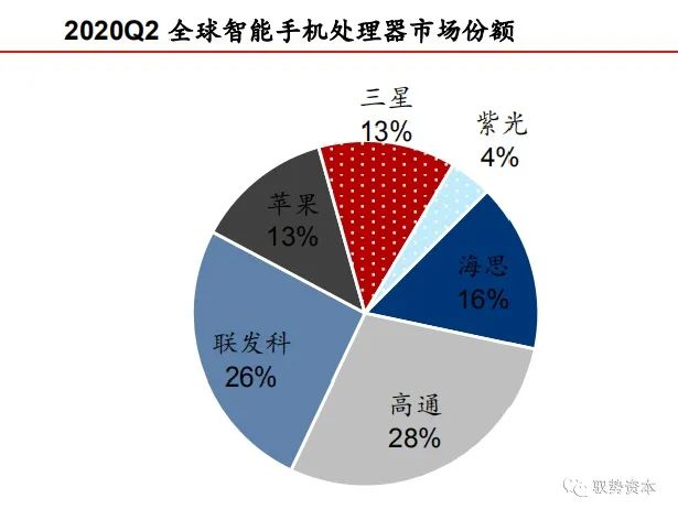
According to the latest data released by CINNO Research, in the first half of 2020, the domestic market sold about 140 million smartphones, with Huawei (including Honor) holding a market share of 40.2%. According to a report from market research firm Counterpoint, in Q2 2020, HiSilicon’s Kirin chip occupied 41% of the domestic smartphone chip market share, becoming the first in the country. At the same time, HiSilicon’s Kirin chip’s global smartphone chip market share rose to 16%, surpassing Apple and Samsung. In recent years, Huawei’s smartphones have achieved a dual boost in both quality and quantity, especially flagship phones gaining widespread recognition in the global market. Aside from the global pandemic and the surge in domestic consumption due to U.S. suppression, we believe the underlying reason is the improvement in user experience gained through hardware-based independent innovation and the formation of differentiated competitive advantages. The Kirin chips self-developed by Huawei, based on ARM processors, are one of the core components of a series of hardware innovations.
The semiconductor industry’s fabless + foundry + OSAT division of labor has achieved the success of HiSilicon chips, including Kirin chips. Huawei’s continuous and substantial investments in HiSilicon have successfully matched the chip design capabilities with the world’s most advanced process and packaging technologies. In the chip design field, ARM’s processor IP licensing model has become one of the important factors for the success of Kirin chips through generations. The positive impact of ARM’s licensing model on Kirin chips includes: First, during the early startup phase, ARM’s licensing model can help latecomer HiSilicon directly reach the same level of processor core performance as competitors in the Android camp. Second, ARM’s dominant position in the smartphone field allows HiSilicon’s self-developed smartphone chips to quickly enter the mainstream smartphone market with the help of ARM’s complete ecosystem. Third, based on the characteristics of the consumer electronics market, ARM’s processor licensing effectively shortens the development cycle and costs for companies, including HiSilicon.
In addition to developing chips based on ARM’s public core architecture, Huawei has also developed the capability to develop processor cores based on the ARM instruction set architecture. HiSilicon has officially stated in the release and configuration table of the Kirin 990 that it uses a core based on A76 (A76 Based), indicating that HiSilicon has a deep understanding of ARM processor cores and instruction sets, mastering the ability to modify the architecture independently. In January 2019, Huawei further released the self-developed server chip Kunpeng 920. This server chip is equipped with 64 HiSilicon self-developed Taishan cores based on the ARMv8 architecture, improving overall server performance by 20% compared to existing market competitors. In May 2019, Huawei announced that it had obtained permanent licensing for the ARMv8 architecture and emphasized that HiSilicon has the capability to continuously develop and design processors based on the ARM licensed architecture.
In recent years, domestic smart terminal SoC chips beyond smartphones have gradually achieved domestic replacement with the help of Cortex-A series processor IP.
Domestic SoCs equipped with ARM architecture processors cover smart HD set-top boxes, IPCs, network cameras, and automotive entertainment information devices. According to data from the Glen Research Institute, in 2018, HiSilicon and Amlogic (688099, no rating) held 60.7% and 32.6% of the domestic IPTV/OTT set-top box chip market, respectively. In 2013, European chip giant STMicroelectronics held over 30% of the domestic set-top box chip market.
The demand for MCUs in the IoT era is increasing, and domestic manufacturers are leveraging ARM Cortex-M to position themselves in the high-end market.
According to IC Insights data, the global sales of MCUs reached $16.4 billion in 2019. Products are mainly used in automotive electronics, industrial control/medical, computer networking, and consumer electronics, with respective market shares of 33%, 25%, 23%, and 11%. IC Insights also predicts that after experiencing a decline in 2019 and 2020, the MCU market will see a mild recovery in 2021, with sales expected to grow by 5% to $15.7 billion, followed by an 8% year-on-year growth in 2022 and an 11% growth in 2023. By then, MCU revenue is expected to reach a new high of $18.8 billion. The global MCU market is mainly occupied by Renesas Electronics (Japan), NXP (Netherlands), Infineon (Germany), Microchip Technology (USA), Samsung Electronics (Korea), STMicroelectronics (ST), and Cypress (USA).
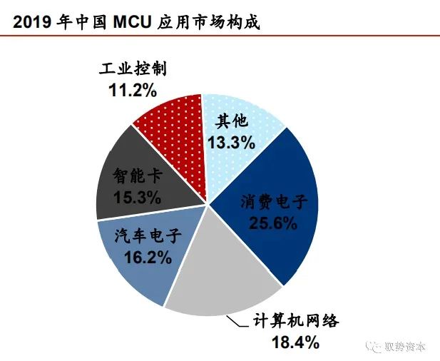
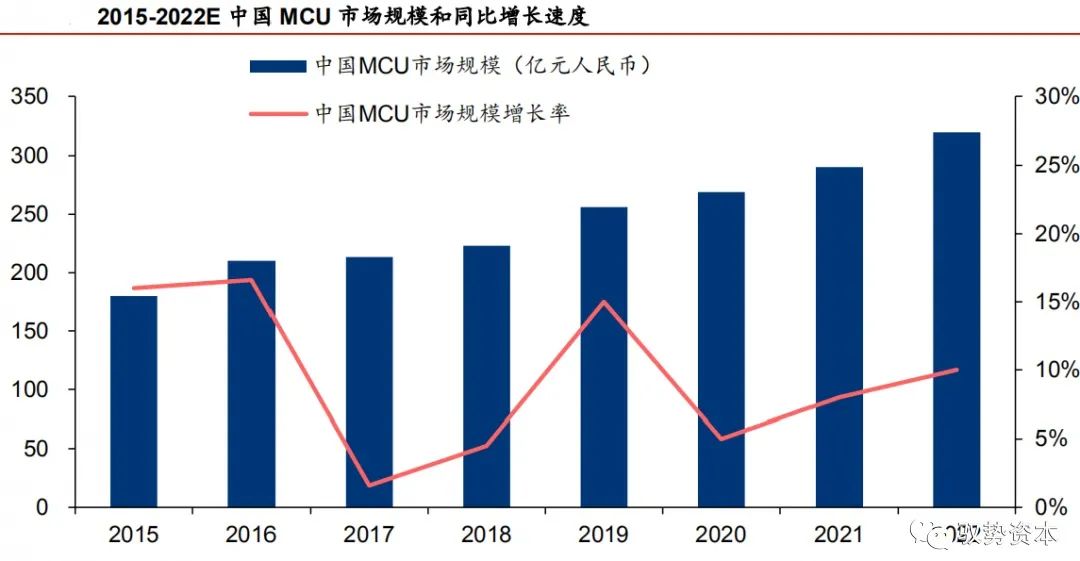
According to HIS and ASPENCORE data, the size of the MCU market in China reached 25.6 billion yuan in 2019. The Chinese MCU application market is mainly concentrated in home appliances/consumer electronics, computer networking, automotive electronics, smart cards, and industrial control, with respective market shares of 25.6%, 18.4%, 16.2%, 15.3%, and 11.2%. Benefiting from the growth of the domestic IoT and new energy vehicle industries, which are leading globally, the size of China’s MCU market has grown at a CAGR of 7.2% from 2008 to 2018, outperforming the global average. At the same time, HIS predicts that by 2022, China’s MCU market size will reach 31.9 billion yuan, with growth continuing to exceed the global average. It is estimated that the sales of domestic MCU manufacturers will reach 14.8 billion yuan in 2020, accounting for 55% of the entire Chinese MCU market.
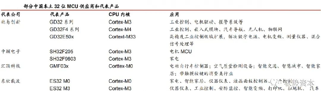
ARM Cortex-M processors help domestic manufacturers position themselves in the upstream value chain of the MCU market. Currently, domestic MCU manufacturers have achieved domestic replacement in mid-to-low-end application fields such as consumer electronics, smart cards, and water, electricity, and gas meters. As the demand for IoT terminals advances, the increasing complexity of tasks in the IoT era will require MCUs to shift towards 16 or 32-bit designs. The 32-bit MCU is the market development direction for the future IoT. The ARM Cortex-M series processors, which meet the above requirements while having rich ecosystem resources, have become the dominant core in the 32-bit MCU market. Domestic MCU manufacturers such as GigaDevice and Zhongying Electronics are actively laying out the domestic mid-to-high-end market based on the ARM Cortex-M series processors, positioning themselves upstream in the industrial value chain. Domestic 32-bit MCUs have begun to enter the high-end MCU market traditionally monopolized by foreign manufacturers.
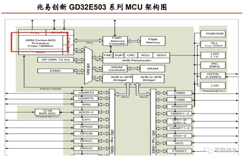
As a leading domestic IC design company, GigaDevice mainly provides 32-bit general-purpose MCU products based on the ARM Cortex-M series. Its GD32 series is a series of general-purpose MCUs based on the ARM® Cortex-M3 and Cortex-M4 cores and is currently the mainstream product in China’s 32-bit general-purpose MCU market, widely used in industrial automation, human-machine interaction, motor control, security, smart home appliances, and IoT fields. According to the company’s mid-2020 report, GigaDevice’s MCU products include over 330 product models, 23 product series, and 11 different packaging types, with cumulative shipments exceeding 400 million units. In July 2020, GigaDevice announced the release of the GD32E5 series high-performance microcontroller based on the new Arm Cortex-M33 core, confirming product routes in wireless connectivity, battery-powered devices, portable and wearable devices, and automotive-grade MCUs.
The ARM acquisition may reshape the global industry landscape, and independent substitution may accelerate.
On September 13, 2020, Pacific Time, American graphics processing and artificial intelligence chip giant NVIDIA (NVDA US, no rating) announced on its official website plans to acquire ARM Limited, the world’s largest processor IP supplier, from Japan’s SoftBank and SoftBank Vision Fund for a total price of $40 billion in NVIDIA stock and cash. NVIDIA stated that this acquisition aims to combine NVIDIA’s extensive AI technology with ARM’s vast computing ecosystem, making NVIDIA a global leader in AI from cloud, smartphones, PCs, autonomous vehicles, and robotics to edge IoT. NVIDIA also promised to continue ARM’s open licensing model, maintain its neutrality among customers, and leverage NVIDIA’s technology to expand ARM’s IP licensing portfolio. Regardless of how integration occurs, the acquisition of ARM, as the world’s largest processor IP supplier, will reshape the global chip industry landscape.
The Chinese smart IoT market has broad prospects, and ARM licensing remains a win-win choice.
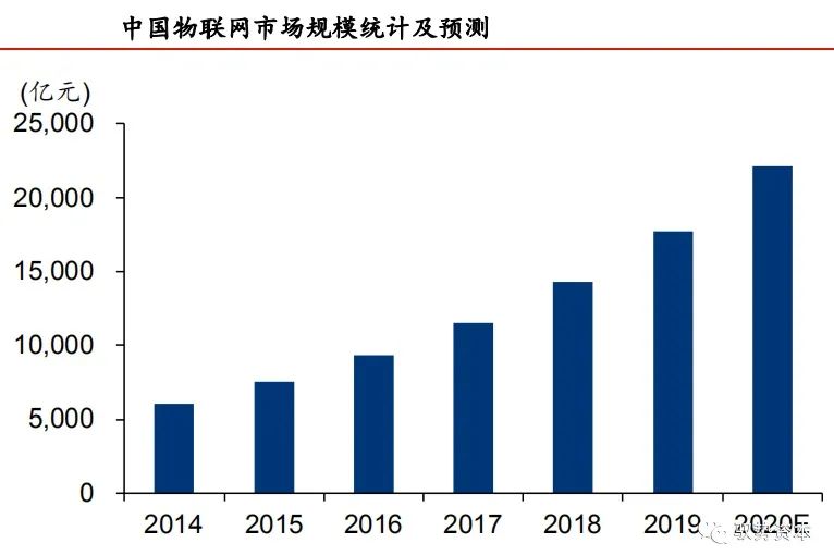
During the 13th Five-Year Plan period, China’s IoT market has steadily grown, and the future market prospects are optimistic. The China Business Industry Research Institute’s report on “Market Prospects and Investment Opportunities in China’s IoT Industry from 2020 to 2025” predicts that in 2020, China’s IoT market size will exceed 2 trillion yuan, reaching 22,165 billion yuan, with an average annual compound growth rate of 24% during the 13th Five-Year Plan period. According to data from the Ministry of Industry and Information Technology, by the end of June 2018, the number of IoT terminal users nationwide had reached 465 million. It is expected that the popularity of smart consumer devices and the application of artificial intelligence technology will continue to support the steady growth trend of China’s IoT scale in the future.
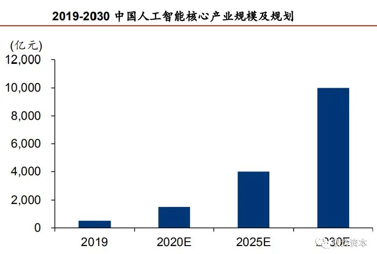
At the same time, China’s artificial intelligence industry is growing rapidly. According to a report released by iiMedia Consulting, the scale of China’s core AI industry is expected to exceed 150 billion yuan in 2020, with a year-on-year growth rate of 26.2%. By June 2020, 24 provinces and cities across the country had released AI industry development plans, of which 18 had set specific industry scale development targets, with the 2020 core industry scale target of these 18 provinces and cities reaching nearly 400 billion yuan, far exceeding the national target of 150 billion yuan.
We believe that as the world’s largest electronics and semiconductor market, China’s domestic chip manufacturers are the most favorable factor in the ARM ecosystem that will not be impacted by the acquisition in the short term. First, for NVIDIA to maintain ARM’s leading position in processor IP licensing, fulfilling ARM’s neutrality commitment is key to success. Second, from both direct commercial benefits and maintaining and expanding ARM’s industrial ecosystem, NVIDIA and ARM will not miss China’s vast smart IoT and artificial intelligence markets. Additionally, due to China’s position in the global market, the approval of China’s antitrust regulatory authorities may be one of the decisive factors for the success of the ARM acquisition. We believe that the two important factors of Sino-US trade friction and the acquisition leading to a significant increase in the concentration of the semiconductor industry may cause the acquisition to undergo more twists and turns in passing China’s antitrust review than the Qualcomm-NXP acquisition in 2018. Academician Ni Guangnan publicly predicted that the Ministry of Commerce of China would veto this acquisition.