
The general basic design process of a PCB is: Preparation –> PCB Structure Design –> PCB Layout –> Routing –> Routing Optimization and Silk Screen –> Network and DRC Check and Structural Check –> Fabrication. Today, we will explore the knowledge of “Preparation”.
Preparation
This includes preparing the component library and schematic. “To do a good job, one must first sharpen their tools.” To create a good board, not only must the design be good, but it must also be well-drawn. Before proceeding with PCB design, it is essential to prepare the component library for the schematic (SCH) and the component library for the PCB. The component library can use the built-in library of Peotel, but it is generally difficult to find suitable components; it is best to create the component library based on the standard size data of the selected components. In principle, the PCB component library should be created first, followed by the SCH component library. The PCB component library has higher requirements as it directly affects the installation of the board; the SCH component library has relatively looser requirements, as long as the pin attributes and connections to the PCB are well-defined.
PCB Component Library
Based on the types and packages of components, the PCB component package library includes the following 11 libraries:1. Integrated Circuits (Through-Hole)2. Integrated Circuits (SMD)3. Inductors4. Capacitors5. Resistors6. Diode Rectifier Components7. Optoelectronic Devices8. Connectors9. Transistors10. Crystals11. Other Components
Schematic Component Library
Based on the types of components, the schematic component library includes the following 16 libraries:1. Microcontrollers2. Integrated Circuits3. TTL74 Series4. CMOS Series5. Diodes, Rectifier Components6. Transistors: including Bipolar Junction Transistors, Field Effect Transistors, etc.7. Crystals8. Inductors, Transformers9. Optoelectronic Devices: including Light Emitting Diodes, Seven-Segment Displays, etc.10. Connectors: including Pin Headers, Ribbon Connectors, Waterproof Plugs and Sockets, etc.11. Electrolytic Capacitors12. Tantalum Capacitors13. Non-Polarized Capacitors14. SMD Resistors15. Other Resistors: including Carbon Film Resistors, Cement Resistors, Photoresistors, Varistors, etc.16. Other Components: including Buzzers, Power Modules, Relays, Batteries, etc.
Establishing the Component Library
In the CIS Project Manager, execute the File/New/Library command to create a new component library in the Library folder of the project manager.
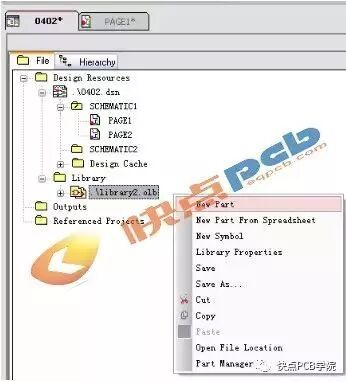
Right-click on the newly created Library component library to edit it, click New Part, and in the pop-up New Part Properties dialog box, define the properties of the new component symbol.
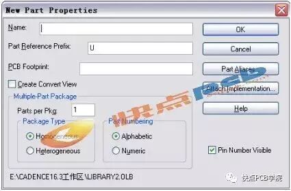
After setting the basic properties, click OK to enter the component editing interface to create the new component symbol.

Under the Place button, you can place component pins, shapes, text, and other attributes, such as creating a DIP20 symbol.
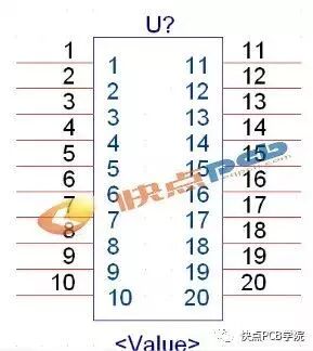
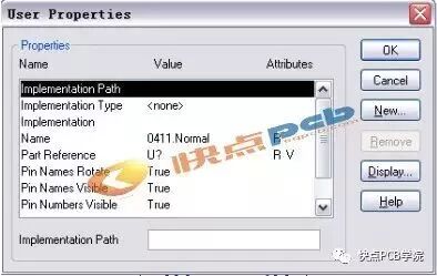
Then double-click the component symbol, and the User Properties dialog box will pop up for editing the component’s properties. You can execute New to add properties, execute Remove to delete component properties, or modify existing properties.

Some screenshots from electronic books
【Complete Set of Hardware Learning Materials】