

With the application of cloud computing, big data, and artificial intelligence technologies, relying solely on CPUs can no longer meet the computational needs of various industries. Scenarios such as massive data analysis, machine learning, and edge computing require a diversified computing architecture, necessitating the collaboration of different processor architectures and heterogeneous computing technologies like GPUs, NPUs, and FPGAs to meet specific algorithm and dedicated computing requirements. Today, I will provide a detailed understanding of FPGA technology.
FPGA stands for Field Programmable Gate Array. It is a product developed further based on programmable devices like PLA, PAL, GAL, and CPLD. As a type of semi-custom circuit in the field of Application-Specific Integrated Circuits (ASIC), it addresses the shortcomings of custom circuits and overcomes the limitations of the number of gate circuits in existing programmable devices.
1. Introduction to FPGA
FPGAs are commonly used to implement digital circuit modules, allowing users to reconfigure the internal logic and I/O modules of the FPGA to meet their needs. They also feature static reprogrammability and dynamic in-system reconfiguration, enabling hardware functionality to be modified through programming like software. It is no exaggeration to say that FPGAs can perform the functions of any digital device, from simple 74 circuits to high-performance CPUs. FPGAs are like a blank sheet of paper or a pile of building blocks, where engineers can freely design a digital system using traditional schematic input methods or hardware description languages.
2. History of FPGA Development
The development history of FPGAs is illustrated in the following figure. Compared to PROM, PAL/GAL, and CPLD, FPGAs offer larger scale and higher performance.

Figure 1: History of FPGA Development
Mainstream FPGA chip manufacturers include Xilinx, Altera, Lattice, and Microsemi, with the first two accounting for a combined market share of 88%. Currently, all mainstream FPGA manufacturers are based in the United States. Domestic FPGAs have started at least 20 years later than those in the US and are still in the growth phase, limited to low-end applications, with no mature applications in the telecommunications market.
In December 2015, Intel acquired Altera for $16.7 billion. Shortly after the acquisition, Altera developed a product roadmap for integrating Intel processors with FPGAs. The benefits of integrating these two products include providing innovative heterogeneous multi-core architectures to meet the demands of new markets such as artificial intelligence while significantly reducing power consumption.

Figure 2: Application History of FPGA in Telecommunications
FPGAs have very mature and widespread applications in aerospace, military, and telecommunications fields. Taking the telecommunications field as an example, during the integrated machine phase of telecommunications equipment, FPGAs were used for network protocol parsing and interface conversion due to their programming flexibility and high performance.
-
In the NFV (Network Function Virtualization) phase, FPGAs achieved a fivefold performance improvement in network element data planes based on general-purpose servers and hypervisors, while also being managed and orchestrated by the general-purpose OpenStack framework.
-
In the cloud era, FPGAs have been used as basic IaaS resources for development and acceleration services in public clouds, with AWS, Huawei, and BAT offering similar general services.
-
As of now, Intel’s Stratix 10 devices have been successfully applied to Microsoft’s real-time artificial intelligence cloud platform, Brainwave.
3. Recent Developments of Two Major FPGA Companies
Xilinx focuses on leading chip technology and a rich array of acceleration solutions, gaining support from mainstream cloud platforms and establishing its leading position in data centers. Its UltraScale+ series FPGAs are over a year ahead of competitors, giving it a competitive edge in cloud platforms, with its VU9P devices widely used in cloud computing platforms of companies including AWS, Baidu, Ali, Tencent, and Huawei.
To meet the increasing performance demands for FPGA chips in the accelerator field, Xilinx has released the next-generation ACAP chip architecture for data centers and launched the 7nm Everest device. This device is no longer a traditional FPGA; it integrates ARM, DSP, and Math Engine processor arrays, and is expected to be mass-produced in 2019. Compared to VU9P, Everest will enhance AI processing performance by 20 times.
Intel, on the other hand, provides a full-stack solution from hardware to platform to applications, avoiding open hardware and platform designs to prevent ecological fragmentation, investing heavily but progressing slowly.
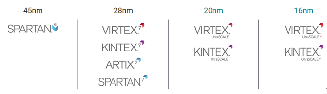
Figure 3: Xilinx Product Series

Figure 4: Intel (Stratix Series as an Example) Product Process Timeline
There are certain technical challenges in the practical application of FPGAs in the data center server market, including the following aspects:
-
1. High programming threshold: Hardware description languages differ from software development languages, requiring developers to have a deep understanding of underlying hardware; thus, talent becomes a significant limiting factor for FPGA applications. Currently, it is estimated that there are about 20,000 people engaged in FPGA development in China.
-
2. High integration difficulty: FPGA development and application require collaboration between software and hardware, including system modeling using high-level languages, hardware code (circuit) design, hardware code simulation, and debugging of low-level driver software with hardware logic.
-
3. Longer development cycle compared to software: Hardware development is more complex than software development, resulting in extended debugging cycles.
-
4. Difficulty in obtaining independent logic IP.
4. Overall Structure of FPGA
The architecture of an FPGA mainly includes Configurable Logic Blocks (CLB), Input Output Blocks (IOB), internal interconnects, and other embedded units.
CLB is the basic logic unit of an FPGA. The actual number and characteristics may vary depending on the device, but each CLB contains a configurable switch matrix made up of 4 or 6 inputs, several selection circuits (multiplexers, etc.), and flip-flops. The switch matrix has high flexibility and can handle combinational logic, shift registers, or RAM when configured.
FPGAs can support many I/O standards, providing ideal interface bridging for system design. The I/Os in the FPGA are grouped by banks, with each bank able to independently support different I/O standards. The most advanced FPGAs currently offer more than ten I/O banks, providing flexible I/O support.
CLBs provide logic performance, while flexible interconnects are responsible for transmitting signals between CLBs and I/Os. There are several types of routing, from those designed specifically for CLB interconnections (short-line resources) to high-speed horizontal and vertical long lines within the device (long-line resources), to global low-skew routing for clocks and other global signals (global dedicated routing resources). Generally, design software from manufacturers hides the interconnect routing tasks, making it significantly easier for users to design.
Embedded hard-core units include RAM, DSP, DCM (Digital Clock Manager), and other specific interface hard cores. The internal structure of FPGA devices is shown in the following diagram.

Figure 5: Internal Structure of FPGA Devices
Generally speaking, the larger the device model number, the greater the scale of logic resources the device can provide. When selecting FPGA devices, users need to refer to this table and comprehensively consider project requirements for logic resources (CLB), internal BlockRAM, interfaces (number of high-speed Serdes), digital signal processing (number of DSP hard cores), and future expansions to choose the most suitable logic device.
5. FPGA Development Process
The FPGA design process involves using EDA development software and programming tools to develop FPGA chips. The typical FPGA development process is illustrated in the following figure, including key steps such as functional definition/device selection, design input, functional simulation, logic synthesis, layout and routing implementation, and programming debugging.
1. Functional definition/device selection: Before starting an FPGA design project, there must be a definition of system functionality and module division. Additionally, it is necessary to weigh the task requirements, such as system functionality and complexity, against speed, device resource availability, cost, and routing feasibility to select an appropriate design scheme and device type.
2. Design input: Design input refers to expressing the designed system or circuit in code using hardware description languages. The most commonly used hardware description language is Verilog HDL.
3. Functional simulation: Functional simulation refers to logically verifying the designed circuit before logic synthesis. Before simulation, a test platform must be set up, and test stimuli prepared. The simulation results will generate report files and output signal waveforms, from which changes in signals at various nodes can be observed. If errors are found, the design must return to modify the logic design. Common simulation tools include ModelSim from Model Tech and VCS from Synopsys.
4. Logic synthesis: Synthesis refers to transforming higher-level abstract descriptions into lower-level descriptions. Synthesis optimization optimizes the generated logic connections based on goals and requirements, flattening hierarchical designs for implementation by FPGA layout and routing software. Currently, synthesis optimization refers to compiling design inputs into a logic connection netlist composed of basic logic units like AND gates, OR gates, NOT gates, RAM, and flip-flops, rather than a real gate-level circuit.
Real gate-level circuits need to be generated using the layout and routing functions of FPGA manufacturers based on the synthesized standard gate-level structure netlist. To convert to a standard gate-level structure netlist, the HDL program must conform to the specific style required by the synthesizer. Common synthesis tools include Synplicity’s Synplify/Synplify Pro software and various synthesis development tools released by FPGA manufacturers.
5. Layout and routing implementation: Layout and routing can be understood as using implementation tools to map logic to the target device structure’s resources, determining the optimal layout for logic, selecting routing channels for linking logic with input/output functions, and generating corresponding files (such as configuration files and related reports); implementation involves configuring the synthesized logic netlist onto a specific FPGA chip. Since only FPGA chip manufacturers have the best understanding of chip structures, layout and routing must use tools provided by chip developers.
6. Programming debugging: The final step of the design is programming debugging. Chip programming refers to generating a data file (bitstream generation) used for loading programming data into the FPGA chip; afterwards, board testing can begin. Finally, the FPGA file (such as .bit file) is downloaded from the computer to the FPGA chip on the board.
6. How to Use FPGA
Once FPGA development is completed, the validated loading file is obtained. After outputting the loading file, normal business processing and validation can begin (using software loading as an example to describe the entire process).
-
1. Logic loading;
-
2. After loading logic, the single board software needs to reset the logic;
-
3. After resetting, the software must wait for a period until the logic phase-locked loop stabilizes;
-
4. The software performs self-check operations on the logic’s external RAM, internal Block RAM, DDRC, etc.;
-
5. After completing self-checks, the software initializes all writable RAM spaces and registers for the logic;
-
6. Once initialization is complete, the software configures table items and registers based on the logic chip manual;
-
7. Once the logic is ready, business processing can commence.
7. Suitable Scenarios for FPGA
FPGAs are suitable for irregular, concurrent, and intensive computation scenarios, as well as protocol parsing processing, including acceleration in fields such as artificial intelligence, gene sequencing, video encoding, data compression, image processing, and network processing.
Content sharing ends here. More exciting server content has been compiled into the electronic book “Comprehensive Knowledge of Data Center Servers,” which consists of 190 pages and is divided into 18 chapters. The brief table of contents is as follows (for detailed directory and content, please refer to the “Read Original” link).
Table of Contents
1.1 Introduction to ARM Processors and Manufacturers 2
1.1.1 Recent Advances in ARM Processor Architecture 8
1.1.2 Main Players in ARM Processors 10
1.1.3 Industry Attitudes Towards ARM Technology Development 10
1.2 Introduction to RISC-V Processors and Manufacturers 11
1.3 Introduction to MIPS Processors and Manufacturers 15
1.3.1 Loongson Products and Recent Developments 15
1.4 Introduction to Alpha Processors and Manufacturers 17
2.1 Overview of Processor Software Stack Architecture 19
2.2 Operating Systems and Pre-installed Software Stacks 20
2.2.1 Introduction to Native Operating System Support 20
2.2.2 Pre-installed Applications for Operating Systems 20
2.3 General Application Porting Analysis 20
2.3.1 Porting of Interpreted Language Applications 21
2.3.2 Porting of Compiled Language Applications 21
2.3.3 Application Installation Packages 22
2.3.4 Differences and Solutions for ARM and X86 Compilation 22
2.3.5 Improving Application Concurrency 24
>>> The Following is a Brief Table of Contents <<<
13. Fundamentals of Fiber Optics and Connectors 97
14. Fundamentals of Fiber Optic Switches 123
15. GPU Architecture and Related Knowledge 135
16. FPGA Architecture and Related Knowledge 179
17. Introduction to Operating System Basics 186
18. Fundamentals of Server Security 196
For more Architectural Technology knowledge, please refer to the electronic book “Comprehensive Collection of Architectural Technology Materials (All)” (which includes 32 technical materials and detailed directories and content can be obtained through the “Read Original” link).
Warm Reminder:
Please scan the QR code to follow the official account, and click on the “Original Link” to obtain details about the “Comprehensive Collection of Architectural Technology Materials (All)” electronic book.

