In this article, we implement a design for interconnecting the ZYNQ FPGA PS side processor with the PL side registers, using the Vitis program on Windows to control the FPGA PS side ARM to read and write the PL side registers.
1. Generate the hardware logic on the PL side
Taking the ZU7EV series as an example, add the PS processor, AXI BRAM controller, BRAM, processor reset, and system ILA in the block design, and connect them as shown in Figure 1.1:
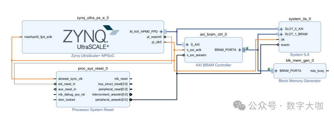
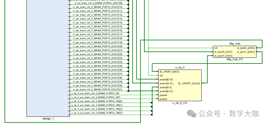
Note that there is a green crawler at the BRAM_PORTA on the right side, which can be debugged or cleared by right-clicking to add or remove tests. We can also implement this by directly adding the ILA IP, but the ILA IP only supports single line connections, making it less convenient than setting up a bus for debugging. The SLOT_1_BRAM of the system ILA in Figure 1 is actually obtained after setting up debugging and running auto connection in the block design.
The address of the AXI BRAM controller in the Address Editor is shown in Figure 1.2:
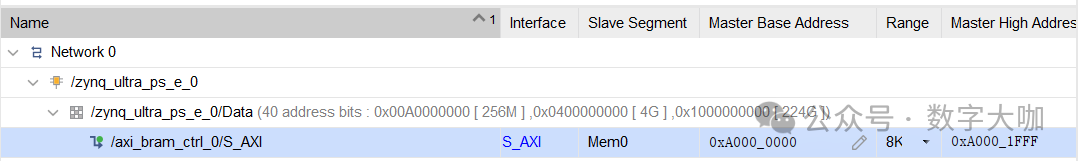
This address will be used when the software accesses BRAM.
The top-level file for calling the block design is as follows:
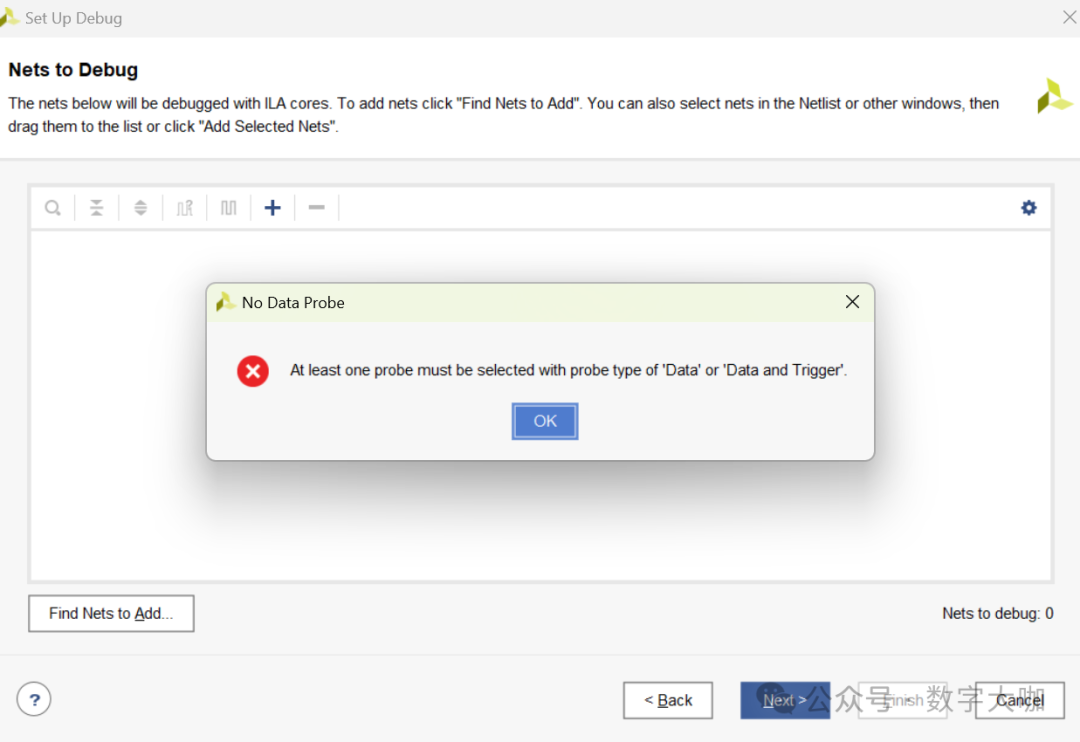
module top();design_1 u0() ; endmoduleWith the top-level file and block design, we can start synthesis. After synthesis is complete, click Set up Debug, and as shown in Figure 1.4, there are no nets that need debugging. In the block design just now, the bus to be debugged has already been added to the design.
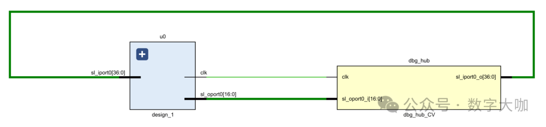
The netlist at this point is shown in Figure 4.
If it was not automatically added in the block design earlier, but instead added through the setup debug method, a u_ila_0 will be added externally to the design, connected to the BRAM interface to be debugged, as shown in Figure 1.5.
Continue to implement, and you can generate the bit file and debug ltx file.
2. Optimize the hardware logic on the PL side
After opening the hardware manager, auto connect, as shown in Figure 2.1.
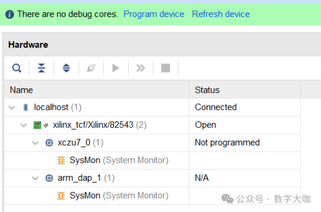
A ZU7 FPGA and an ARM core appeared.
Continue to program the device, and the following warning appears.

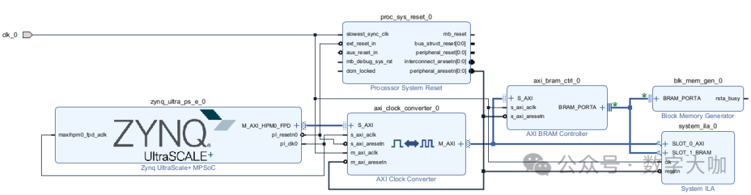
The problem is that the clock we are using is generated by the PS, and the defect in the above project is that the debug clock depends on the operation of the PS side. We can modify this project by disconnecting the clk pin of system ILA from pl_clk0 and setting a port (to use an external clock not controlled by the PS) and adding an AXI clock converter, as shown in Figure 2.2:
After the block design is completed, refer to the clock generation method in the previous UART design and instantiate design_1.
module top( input clk125_p , input clk125_n ); wire clk125,clk ; IBUFDS u_IBUFDS( .O ( clk125), .I ( clk125_p), .IB ( clk125_n)) ; BUFG u_BUFG( .O ( clk ) , .I ( clk125)); design_1 u0(.clk_0(clk)) ; endmoduleIn addition, add clock.xdc under constrs_1 as follows:
set_property IOSTANDARD LVDS [get_ports clk125_n] set_property PACKAGE_PIN H9 [get_ports clk125_p] set_property PACKAGE_PIN G9 [get_ports clk125_n] set_property IOSTANDARD LVDS [get_ports clk125_p]Reimplement to generate the bit file and debug ltx file.
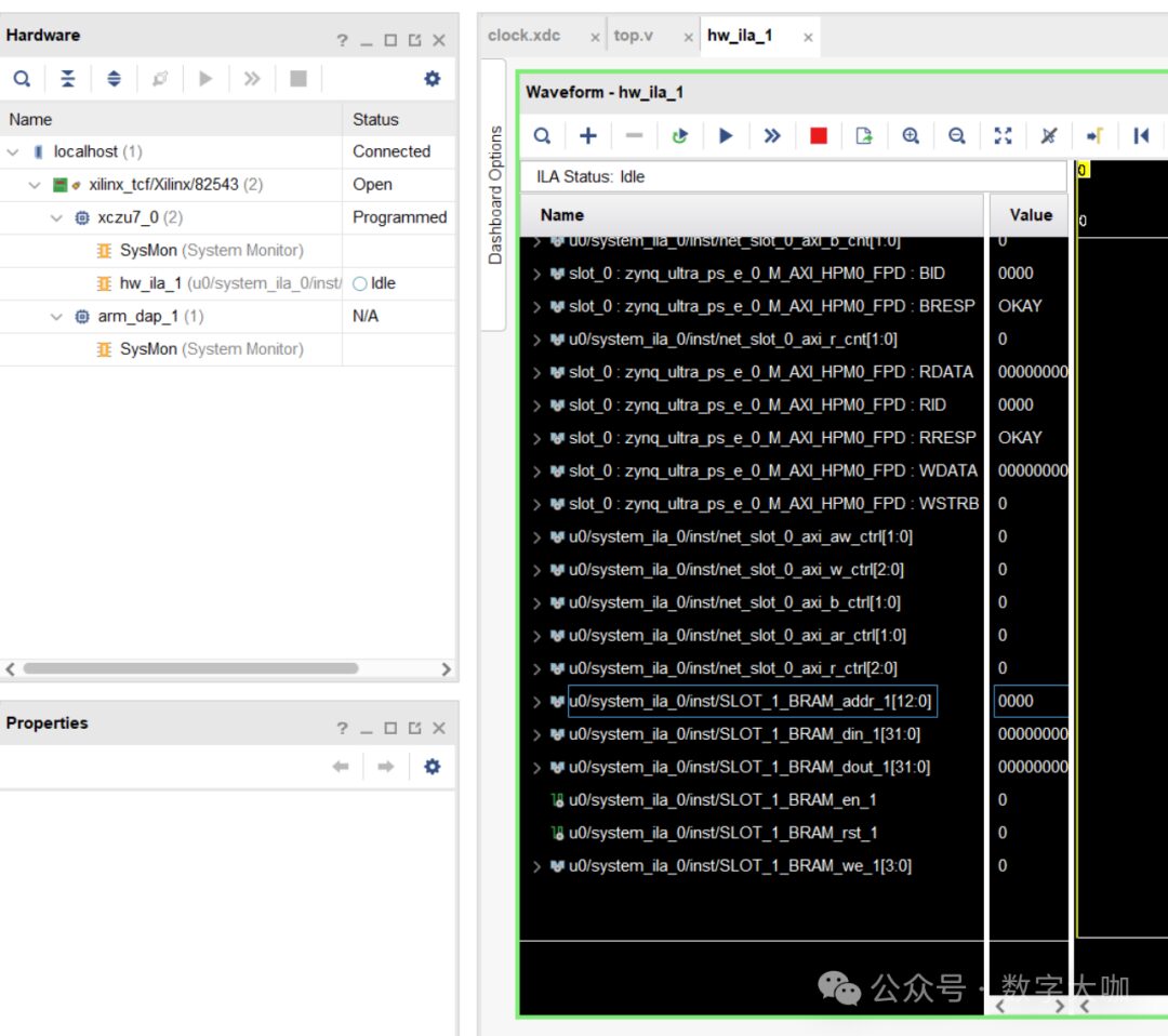
After opening the hardware manager, auto connect, this time the debugging window in Figure 2.3 appears successfully.
3. Generate the software logic on the PS side
First, export the hardware, in Vivado go to File->Export->Export Hardware Platform as shown in Figure 3.1.
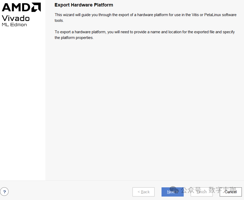
Select Pre-synthesis, then Next as shown in Figure 3.2.
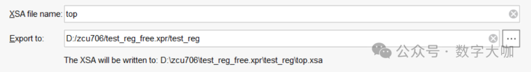
Finally, generate the xsa file as shown in Figure 3.3.

Next, start writing the PS program.
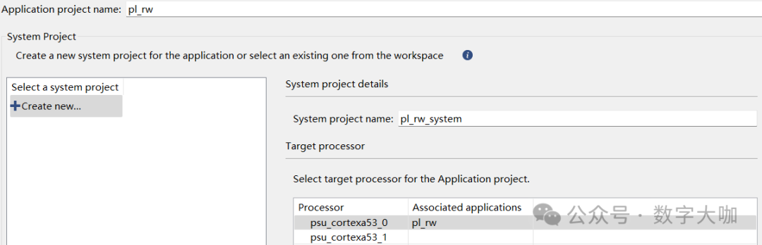
Open Vitis and create an application project as shown in Figure 3.4.
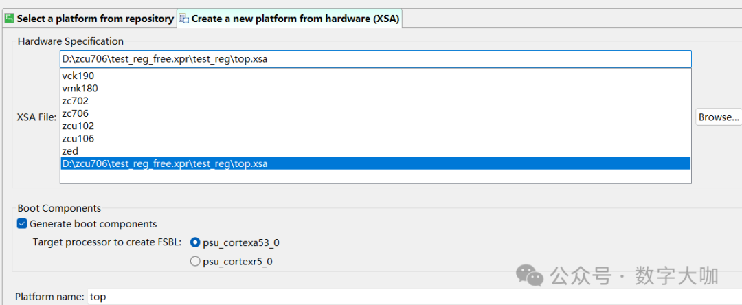
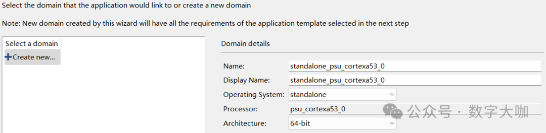
Then use the exported xsa to create a new platform as shown in Figure 3.5.
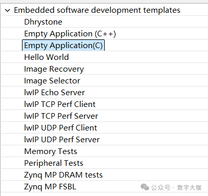
Finally, select an empty C project and finish creating it as shown in Figure 3.8.
After creation, the Vitis IDE is shown in Figure 3.9.
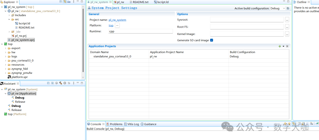
The entire interface contains a lot of information, with a focus on the Explorer on the left side, which contains detailed information about the project. Note that the src of pl_rw_system->pl_rw is where we place our software program. The lscript.ld is placed there by default, used for linking the application program, with the hardware configuration addresses pre-set, which are obtained from the previous top.xsa file.
Write the software code and header files as follows:
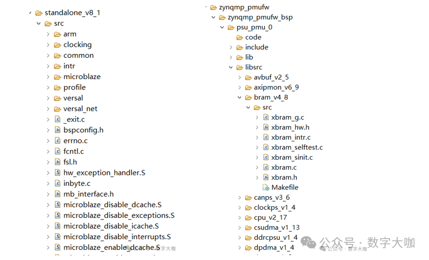
#include "xil_printf.h"#include "xbram.h"#include <stdio.h>#include "rw.h"int main(){ u32 Write_Data = 0 ; int i ; int Read_Data ; xil_printf("Hello!\r\n") ; xil_printf("Bram write start!\r\n") ; for(i=0; i<1;i=i+1) { XBram_WriteReg(XPAR_BRAM_0_BASEADDR, i , Write_Data+0x5A) ; Write_Data += 1 ; } xil_printf("Bram read start!\r\n") ; for(i=0; i<1;i=i+1) { Read_Data = XBram_ReadReg(XPAR_BRAM_0_BASEADDR , i) ; xil_printf("Address is %d\t Read data is %d\t\n", i/4 ,Read_Data) ; } return 0 ; }#ifndef PL_BRAM_CTRL_H#define PL_BRAM_CTRL_H /****************** Include Files ********************/#include "xil_types.h"#include "xstatus.h" #define PL_BRAM_CTRL_S00_AXI_SLV_REG0_OFFSET 0 #define PL_BRAM_CTRL_S00_AXI_SLV_REG1_OFFSET 4 #define PL_BRAM_CTRL_S00_AXI_SLV_REG2_OFFSET 8 #define PL_BRAM_CTRL_S00_AXI_SLV_REG3_OFFSET 12 #define XPAR_BRAM_0_BASEADDR 0xA0000000 #define PL_BRAM_CTRL_mWriteReg(BaseAddress, RegOffset, Data) \ Xil_Out32((BaseAddress) + (RegOffset), (u32)(Data)) #define PL_BRAM_CTRL_mReadReg(BaseAddress, RegOffset) \ Xil_In32((BaseAddress) + (RegOffset)) XStatus PL_BRAM_CTRL_Reg_SelfTest(void * baseaddr_p); #endif // PL_BRAM_CTRL_HSelect xil_printf.h, xbram.h, and right-click to select open declaration, we can see that these header files belong to standalone_v8_1 and the bram library inside pmu, as shown in Figure 3.10.
In assistant->pl_rw->Debug, right-click build as shown in Figure 3.11.
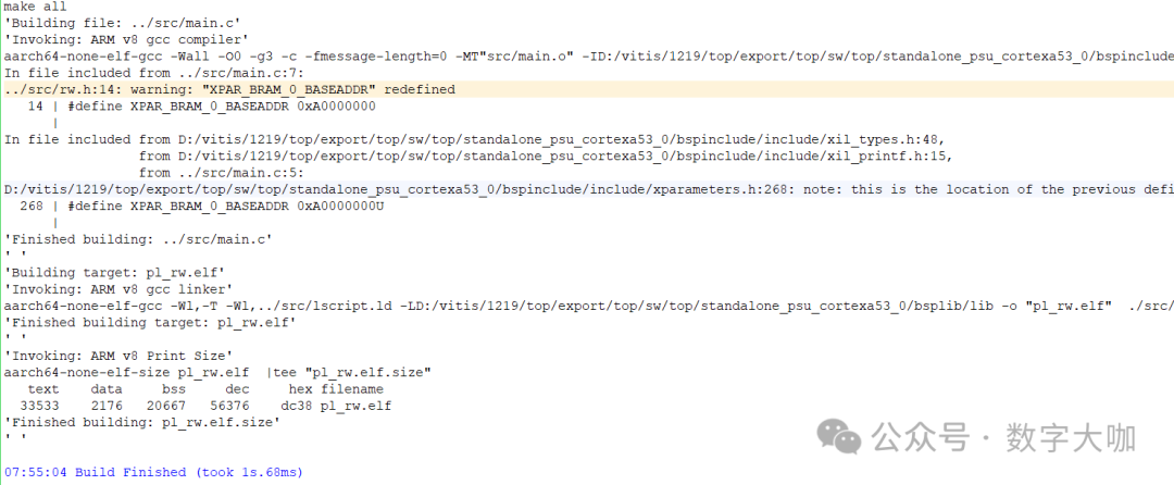
Note that the compiler is using none-elf-gcc, linking file lscript.ld, and producing pl_rw.elf. Friends who are not familiar with compilation can refer to the end of the article on SOC design – instruction chapter.
In assistant->pl_rw_system->Debug, right-click build as shown in Figure 3.12.
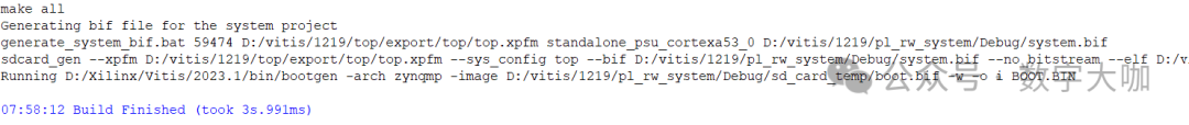
At this point, we can further generate BOOT.BIN for SD card boot.
Connect to the serial port software to receive the output of xil_printf, click assistant->pl_rw->Debug, right-click run->run configurations to set the location of the program bit file.
Right-click run->launch hardware, the program starts running, downloads the bit file, and enters single-step debugging state 3.13:
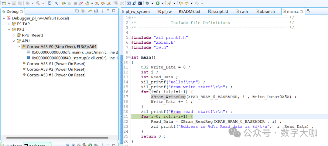
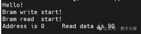
The serial output is as follows and is consistent with expectations 3.14:
This article ends here, and I will continue to share the use of the PS processor. If you like this article, please follow the author.
The reference project and “Course_s2_ALINX_ZYNQ_MPSoC Development Platform Vitis Application Tutorial V1.01” have been shared via cloud drive.
Link: https://pan.baidu.com/s/1nZAwqJeZaCSrN08UyQo3HQ Extraction code: n2ge
–Shared by Baidu Cloud Super Member v6
SOC Design (1) – Understanding Instruction Set
Xilinx IP Introduction (5) – PS Processor-1
Xilinx IP Introduction (4) – System ILA
Xilinx IP Introduction (3) – GTH Transceivers
Xilinx IP Introduction (2) – DDR4 SDRAM (MIG)
Xilinx IP Introduction (1) – PCIe XDMA