Chip Design in the Semiconductor Subsector

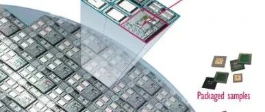
Today, let’s talk about chip design. The production of chips involves three core steps: design, manufacturing, and packaging/testing.In simple terms, chip design is about drawing circuit diagrams on silicon wafers, but it is not done directly on the wafers. The software used for this is EDA (Electronic Design Automation) software, which is mainly monopolized by … Read more