Today, let’s talk about chip design. The production of chips involves three core steps: design, manufacturing, and packaging/testing.In simple terms, chip design is about drawing circuit diagrams on silicon wafers, but it is not done directly on the wafers. The software used for this is EDA (Electronic Design Automation) software, which is mainly monopolized by foreign companies. After the design is completed, a photomask (similar to a camera film) is produced, and strong light passes through the photomask to project the circuit onto the silicon wafer (the intermediate process is very complex, so I won’t elaborate). The excess photoresist is etched away, leaving the circuit on the thin film. A single chip can have dozens of layers of circuit diagrams, and the above photolithography process is repeated to draw layer by layer of circuits onto the silicon wafer.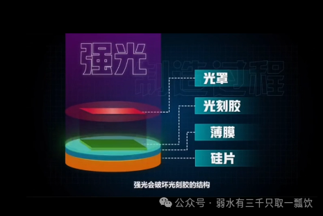 The cost of chip design is highly dependent onprocess nodes (such as 28nm, 7nm, 3nm),chip types (such as consumer SoCs, automotive chips, AI chips), anddesign scale (such as the number of transistors and functional complexity), ranging from millions to billions of dollars. Its cost structure can be broken down into “fixed core costs” and “variable/implicit costs.”
1. Core Cost Structure of Chip Design (by Process Breakdown)
The chip design process from “requirements definition” to “tape-out verification” focuses core costs onIP licensing, tool software, tape-out, and verification testing, with cost differences across different process nodes exhibiting exponential growth.
1. Fixed Costs: Do not vary with production scale, representing the “threshold cost” for design initiation
|
Cost Segment |
Core Content |
Cost Range (by Process Node) |
Key Notes |
|
IP Licensing Fees |
Purchasing third-party mature IP (such as CPU cores, GPU architectures, DDR interfaces, PCIe protocol stacks, RF modules, etc.) |
Mature Process (28nm and above): 1 million – 5 million USDAdvanced Process (7nm/5nm): 5 million – 20 million USDLeading Process (3nm/2nm): 20 million – 50 million USD |
Self-developed IP costs more (for example, Apple’s self-developed M series CPU IP development costs hundreds of millions), while small and medium design companies generally rely on third-party IP (such as ARM’s Cortex series) |
|
EDA Tool Fees |
Purchasing full-process EDA software (such as simulation, synthesis, layout, and physical verification tools from Synopsys, Cadence, Mentor) |
Mature Process: 2 million – 8 million USD/yearAdvanced Process: 8 million – 30 million USD/yearLeading Process: 30 million – 80 million USD/year |
EDA tools are charged on a “subscription basis,” and advanced processes require additional purchases of specialized tools such as “photolithography compatibility analysis” and “quantum effect correction,” which can double costs |
|
Labor Costs |
Engineer team salaries (for front-end design, back-end physical implementation, verification, DFT, layout, etc.) |
Mature Process (50-100 person team): 5 million – 15 million USD/yearAdvanced Process (150-300 person team): 15 million – 50 million USD/yearLeading Process (300+ person team): 50 million – 150 million USD/year |
Core engineers (such as 7nm physical implementation experts) generally earn over 500,000 USD annually, and team size increases linearly with process complexity (3nm design requires over 50% more manpower than 7nm) |
2. Variable/One-time Costs: Directly related to design verification and mass production preparation
-
Tape-out Costs: The cost of delivering design data to the wafer fab to produce the “first version chip,” which is the “largest one-time expenditure” in the design phase.
- Mature Process (28nm): Single tape-out costs approximately 500,000 – 2 million USD (based on 8-inch/12-inch wafers, with 10-20 test chips);
- Advanced Process (7nm): Single tape-out costs approximately 10 million – 30 million USD (EUV lithography costs are high, requiring multiple rounds of optimization, with some designs needing 3-5 rounds of tape-out);
- Leading Process (3nm): Single tape-out costs over 50 million USD, with some complex AI chips (such as GPUs) costing 100 million – 200 million USD (requiring customized lithography solutions).Note: The failure rate for tape-out is high (the success rate for the first version of advanced processes is less than 50%), and multiple rounds of tape-out can directly double costs.
-
Verification and Testing Costs: Ensuring that the chip meets functional, performance, and reliability standards, including:
- Simulation Testing: Building a hardware simulation platform (such as Synopsys Zebu), costing approximately 2 million – 10 million USD;
- Prototype Verification: Creating FPGA prototype boards (such as Xilinx UltraScale), costing approximately 500,000 – 3 million USD;
- Mass Production Testing: Designing test vectors (DFT), purchasing testing equipment (ATE), costing approximately 1 million – 5 million USD (the larger the mass production scale, the lower the amortized cost of testing equipment).
2. Cost Comparison of Design Across Different Process Nodes (2024 Industry Data)
Upgrading process nodes leads to a dramatic increase in “physical effect complexity” (such as line delay, crosstalk, quantum tunneling), which in turn drives up costs for IP, EDA, labor, and tape-out, with specific differences as follows:
|
Process Node |
Typical Chip Types |
Total Design Cost (from initiation to mass production preparation) |
Core Cost Drivers |
|
28nm (Mature) |
IoT chips, automotive MCUs, power management ICs |
10 million – 30 million USD |
Low IP costs (mostly general interfaces), EDA tools do not require specialized functions, small team size (under 50 people) |
|
14nm (Mid-range) |
Mid to high-end mobile SoCs, server CPUs, mining chips |
30 million – 100 million USD |
Need to introduce FinFET structure-related IP, EDA tools require physical verification tool upgrades, tape-out costs exceed 5 million USD |
|
7nm (Advanced) |
High-end mobile SoCs (such as Snapdragon 8 Gen3), AI acceleration chips (such as NVIDIA A100) |
100 million – 500 million USD |
Dependent on EUV lithography IP, EDA tool costs exceed 20 million USD, tape-out requires 3-4 rounds (costing over 20 million USD/round), team size exceeds 200 people |
|
3nm/2nm (Leading) |
Flagship AI chips (such as NVIDIA H100), self-developed high-end SoCs (such as Apple M4) |
500 million – 2 billion USD |
Need customized CPU/GPU IP, EDA requires quantum effect correction tools, tape-out costs exceed 50 million USD/round, verification cycles exceed 2 years |
Foreign chip design companies include:
|
Company |
Headquarters |
Model |
Core Positioning |
Typical Products / Technologies |
|
NVIDIA |
USA |
Fabless |
GPU and AI computing |
Hopper/H100/H200, CUDA ecosystem |
|
AMD |
USA |
Fabless/IDM |
CPU+GPU/APU |
Ryzen, Epyc, RDNA GPU |
|
Qualcomm |
USA |
Fabless |
Mobile and IoT |
Snapdragon SoCs, 5G modems |
|
Broadcom |
USA |
Fabless |
Networking and communication |
Ethernet switches / PHY, wireless connectivity |
|
Marvell |
USA |
Fabless |
Storage / Networking / Wireless |
SSD controllers, WiFi / Ethernet controllers |
|
Texas Instruments |
USA |
IDM |
Analog and embedded |
Power management, signal chain, MCUs |
|
NXP |
Netherlands |
Fabless/IDM |
Automotive and IoT |
Body control, ADAS / in-vehicle networking |
|
Infineon |
Germany |
IDM |
Power and automotive electronics |
MOSFET/IGBT, automotive microcontrollers |
Domestic chip design companies include:
|
Company |
Headquarters |
Model |
Core Positioning |
Typical Products / Technologies |
|
Huawei HiSilicon Hisilicon |
Shenzhen |
Fabless |
Comprehensive SoCs and AI |
Kirin / Ascend / Kunpeng, 5G modems |
|
UNISOC UNISOC |
Shanghai |
Fabless |
Communication and platform-type SoCs |
4G/5G mobile and IoT platforms |
|
Cambricon Cambricon |
Beijing |
Fabless |
AI chips (cloud/edge) |
NPU architecture and acceleration chips |
|
Horizon Horizon |
Beijing |
Fabless |
In-vehicle AI / Autonomous driving |
Journey series SoCs |
|
Montage Montage |
Shanghai |
Fabless |
Memory interfaces / Interconnects |
DDR5 memory buffers / training chips |
|
GigaDevice GigaDevice |
Beijing |
Fabless |
MCUs and storage |
NOR Flash, GD32 MCUs |
|
SGMicro SGMicro |
Beijing |
Fabless |
Analog / Mixed-signal |
Power management, high-precision ADC / operational amplifiers |
|
Allwinner Allwinner |
Zhuhai |
Fabless |
Consumer and IoT SoCs |
Multimedia / Low-power application processors |
|
Rockchip Rockchip |
Fuzhou |
Fabless |
Consumer and visual SoCs |
Smart hardware / Tablet / Box platforms |
|
GK GK |
Changsha |
Fabless |
Video / Storage / Security |
Video encoding / Storage controllers / Security chips |
|
Shanghai Zhaoxin |
Shanghai |
Fabless |
x86 general computing |
x86 CPUs/SoCs |
|
Haiguang Information |
Tianjin |
Fabless |
x86 server CPUs |
Haiguang x86 processors |