In the field of semiconductor chip manufacturing, MPW (Multi-Project Wafer), or Multi-Project Wafer, is a collaborative model that combines multiple different design projects onto the same wafer for manufacturing. This model is particularly suitable for companies, universities, and research institutions with limited R&D budgets, significantly lowering the economic threshold for single wafer runs through a cost-sharing mechanism.
The Core Mechanism of MPW
The core of MPW lies in the shared cost of the mask set. In advanced process nodes, the cost of mask sets is extremely high. For example, at the 28 nm process node, a set of masks costs about $3-5 million, while at 7 nm, it can exceed $10 million. MPW reduces costs by dividing the entire mask set into multiple “slots” for different users, thus sharing the costs among dozens of participants, significantly lowering the expenditure for each.
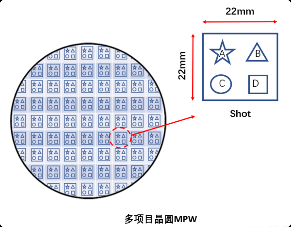
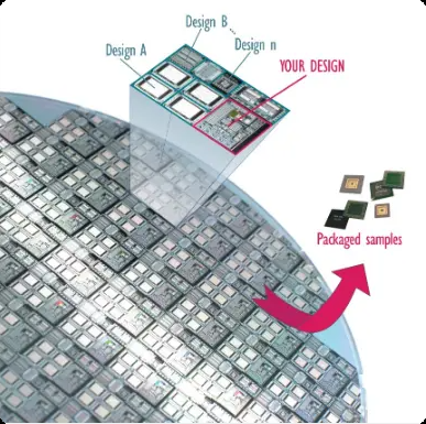
In addition to the mask costs, the actual utilization efficiency of the wafer itself is also improved. A single wafer can typically produce hundreds or even thousands of chips; if it is solely occupied by a single project, excess capacity will be wasted. MPW allows multiple designs to share the physical space of the wafer, distributing fixed manufacturing costs, enabling prototype validation or academic research projects to obtain actual chip samples at a very low cost.
The Technical Process of MPW
The MPW process begins with design submission and compilation. Participants must complete the GDSII files for circuit layouts in advance and submit them to the MPW service organization within the specified time. This organization will perform basic rule checks (DRC/LVS) on the designs but will not verify whether the functionality is correct—if there are logical errors in the design, the manufactured chips will be unusable.
Next is mask production and photolithography. The service provider will integrate and arrange all submitted designs on the mask to maximize the utilization of the wafer area. During this process, the foundry’s requirements for wafer utilization density (usually not less than 85%) must also be met; unoccupied areas will be filled with structures (such as test circuits or redundant units).
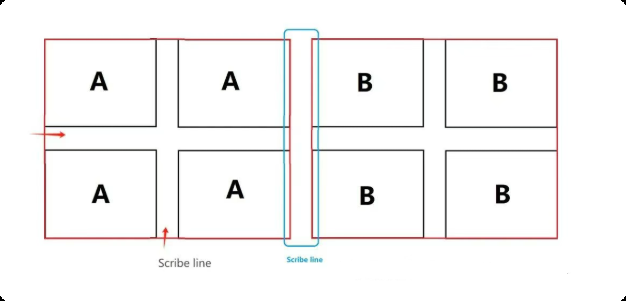
The manufacturing stage uses uniform process parameters. All projects must be based entirely on the same process node, device model, and PDK (Process Design Kit); different derivative versions (such as low power and ultra-low power) cannot be mixed. After multiple processes such as photolithography, etching, and deposition, the physical structures of all circuits are formed on the wafer.
The final stage is wafer cutting and distribution. After testing, the completed wafer is cut into individual dies and distributed to each participating team according to the number of slots occupied by the project. It should be noted that MPW services typically do not guarantee the yield of a single project; if the chips are completely lost due to design issues, the costs will not be refunded.
Target Audience for MPW
The MPW model primarily serves the following groups:
Academic institutions and research organizations: Used for experimental circuit design validation to obtain physical chips at a lower cost, promoting research progress;
Startups and small enterprises: Can complete prototype testing and functional optimization through MPW before investing in large-scale production, significantly reducing R&D risks and financial pressure;
IP development and verification teams: Used to verify the actual performance and process compatibility of intellectual property modules.
This model is particularly suitable for small-batch pilot production, multiple design iterations, and process verification projects, significantly shortening the cycle from design to sample and accelerating the product launch process.
Challenges Faced by MPW
Despite the significant cost and efficiency advantages of MPW, there are several technical and management challenges:
Process deviation is a major concern. MPW often uses engineering lots for wafer runs, and the electrical parameters of the devices may differ by ±10% from production lots, which can significantly impact the performance of analog or RF circuits.
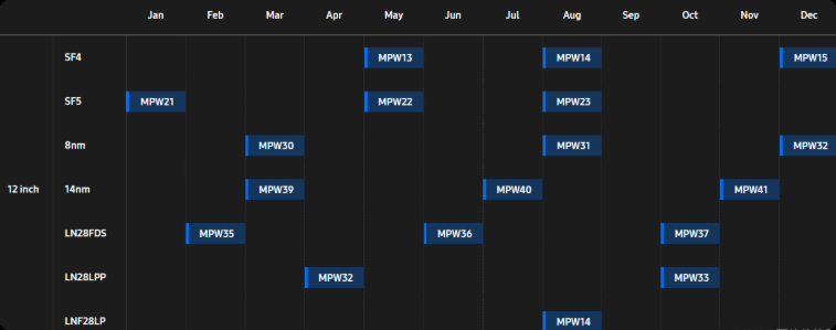
Time coordination difficulties are a common operational bottleneck. MPW is generally planned to open quarterly or semi-annually, and design submissions have strict deadlines. Any delays may require waiting for the next round, thus extending the product development cycle.
Insufficient packaging and testing support is also noteworthy. MPW services typically only provide bare dies, and subsequent tasks such as wire bonding, packaging, and testing must be arranged by the user. The unit price of small-batch packaging orders may reach ten times that of mass production prices, further increasing overall costs and complexity.
Additionally, all designs must comply with the technical requirements of the same process node, and different projects cannot mix process versions, limiting the participation of certain special designs.
Development Trends of MPW
Currently, MPW services are also continuously evolving to meet the new demands of the semiconductor industry. On one hand, advanced process nodes (such as 3nm, 5nm) and AI chips have become popular options for MPW; for example, some companies are planning to use the MPW model to validate their self-designed AI accelerator chips on high-end processes to reduce dependence on traditional suppliers.
On the other hand, with the rise of Chiplet and 2.5D/3D packaging technologies, MPW is also expanding its collaboration forms. Multiple functional modules can be manufactured on the same wafer and then integrated through advanced packaging, achieving a higher level of system integration and performance optimization.
On the service provider side, mainstream foundries (such as TSMC, Samsung, and SMIC) and cooperative channels all offer MPW services and are gradually improving supporting toolchains, such as online quoting systems, cutting simulation tools, and porting kits, to assist users in efficiently completing the entire process from design to sample.
As a key innovation-driving mechanism in the semiconductor ecosystem, MPW significantly lowers the threshold for chip manufacturing through resource sharing and cost distribution. Especially for resource-limited small and medium teams and academia, it provides an important avenue to access advanced processes and achieve technology validation. However, participants must also fully understand its technical constraints and risks, and be well-prepared for process selection, design verification, and project management.