1. Spacing Between SMD Components
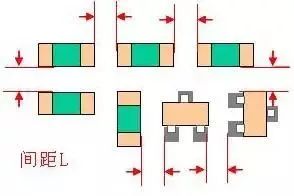
The spacing between SMD components is a crucial issue that engineers must pay attention to during layout. If the spacing is too small, it becomes very difficult to print solder paste and avoid solder bridging.The recommended distances are as follows:
-
Spacing requirements for SMD components:
-
Same type of components:≥0.3mm
-
Different types of components:≥0.13*h + 0.3mm (h is the maximum height difference of nearby components)
-
Spacing requirement for components that can only be manually placed:≥1.5mm
The above suggestions are for reference only and can be adjusted according to each company’s PCB process design specifications.
2. Distance Between Through-Hole Components and SMDs
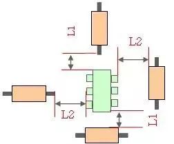
As shown in the image above, a sufficient distance should be maintained between through-hole resistors and SMDs, recommended to be between 1-3mm. Due to processing difficulties, the use of through-hole components is now quite rare.
3. Placement of Decoupling Capacitors for ICs
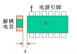
Decoupling capacitors need to be placed near the power pins of each IC, as close to the IC’s power port as possible. When an IC has multiple power ports, decoupling capacitors should be laid out for each port.
4. Component Placement Direction and Distance at PCB Edges
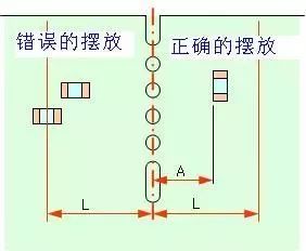
Since PCBs are generally made using panelization, components near the edges must meet two conditions.
The first is to be parallel to the cutting direction (to ensure uniform mechanical stress on the components; for example, if the components are placed as shown on the left in the image, during panel separation, the stress direction on the two solder pads may differ, potentially causing components to detach from the pads).
The second is that no components should be placed within a certain distance (to prevent damage to components during board cutting).
5. Connecting Adjacent Pads
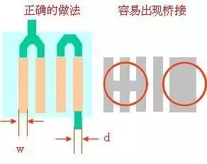
If adjacent pads need to be connected, first ensure that they are connected externally to prevent bridging, and also pay attention to the width of the copper traces at this time.
6. Considering Heat Dissipation for Pads in Regular Areas
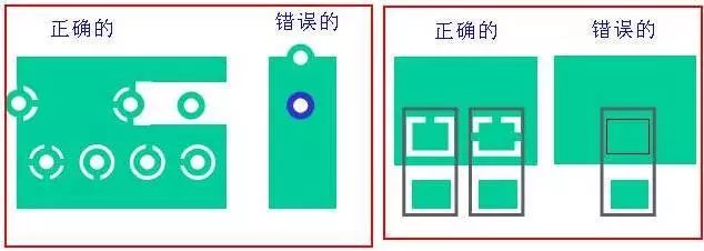
If a pad falls in a copper area, it is recommended to connect the pad to the copper area as shown on the right, and determine whether to connect with one wire or four wires based on the current size.If the method on the left is used, it may be difficult to solder or repair components because the heat disperses through the copper, making it hard to solder.
7. Adding Tear Drops When Leads Are Smaller Than Pads
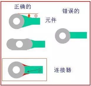
If the lead is smaller than the through-hole pad, a tear drop should be added as shown on the right. Adding a tear drop has the following benefits:
(1) It avoids sudden width changes in signal traces that could cause reflections, allowing for a smoother transition between traces and component pads.
(2) It resolves the problem of connections between pads and traces breaking easily under impact.
(3) It also makes the PCB look more aesthetically pleasing.
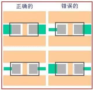
8. Ensure Consistent Width for Leads on Both Sides of Pads
9. Remember to Keep Unused Pins Grounded
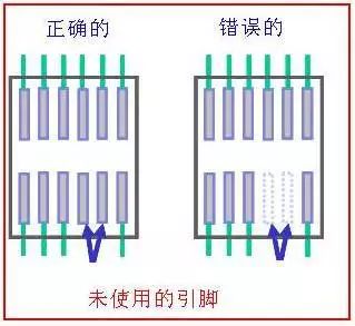
For example, in the image above, two pins of a chip are not used, but the physical pins still exist. If the pins are left floating as shown on the right, they can easily cause interference.Grounding the pads can help avoid interference.
10. Avoid Placing Vias on Pads
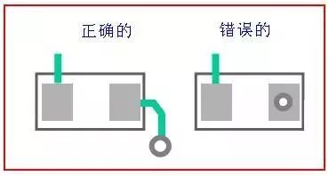
It is best to avoid placing vias on pads, as it can lead to solder leakage and cold solder joints.
11. Maintain Distance Between Wires or Components and Board Edges

It is important that leads or components are not placed too close to the edge of the board, especially for single-sided boards. Single-sided boards are often made of paper, which can easily break under stress. If leads or components are placed at the edges, they can be affected.
12. Ensure Electrolytic Capacitors Are Far from Heat Sources
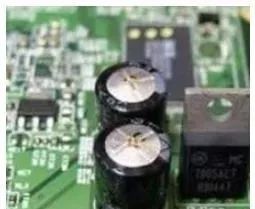
First, ensure that the environmental temperature for electrolytic capacitors meets the requirements, and second, position the capacitors as far away from heat sources as possible to prevent the internal liquid electrolyte from drying out.
Source:21ic Electronics Network, copyright belongs to the original author. If there are copyright issues, please contact us, and we will handle it as soon as possible.

Follow 【PCB Network City】 to receive the latest industry news and gain a competitive edge. The WeChat public platform provides new services for professional PCB networking.