1. Layout
10 Rules for Component Layout:
1. Follow the principle of “large first, small later, difficult first, easy later,” meaning important circuit units and core components should be laid out first.
2. The layout should refer to the schematic diagram, arranging major components based on the main signal flow direction of the board.
3. The arrangement of components should facilitate debugging and maintenance, meaning small components should not be placed around large components, and there should be enough space around components that need debugging.
4. For circuit parts with the same structure, adopt a “symmetrical” standard layout as much as possible;
5. Optimize the layout according to the standards of uniform distribution, center of gravity balance, and aesthetic appearance;
6. Components of the same type should be placed in the same direction in the X or Y direction. Polarized discrete components of the same type should also strive to maintain consistency in the X or Y direction for ease of production and inspection.
7. Heating components should generally be evenly distributed to facilitate heat dissipation for the board and the entire machine, and temperature-sensitive components should be kept away from high-heat components, except for temperature detection components.
8. The layout should strive to meet the following requirements: keep total wiring as short as possible, with key signal lines being the shortest; completely separate high-voltage and high-current signals from low-voltage and low-current weak signals; separate analog signals from digital signals; separate high-frequency signals from low-frequency signals; and ensure sufficient spacing for high-frequency components.
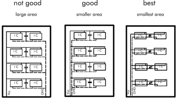
9. The layout of decoupling capacitors should be as close as possible to the IC’s power pins, minimizing the loop formed with power and ground.
10. When laying out components, consider grouping devices using the same power supply together as much as possible for future power separation.
2. Routing
(1) Routing Priority
Key signal lines are prioritized: analog small signals, high-speed signals, clock signals, and synchronous signals should be routed first.
Density priority principle: Start routing from the devices with the most complex connections on the board. Begin routing from the most densely connected areas on the board.
Points to note:
a. Provide dedicated routing layers for clock signals, high-frequency signals, and sensitive signals, ensuring the smallest loop area. If necessary, adopt manual priority routing, shielding, and increased safety spacing methods to ensure signal quality.
b. The EMC environment between the power layer and ground layer is poor; avoid routing interference-sensitive signals.
c. Networks with impedance control requirements should be routed according to line length and width requirements.
(2) Four Specific Routing Methods
1. Clock Routing:
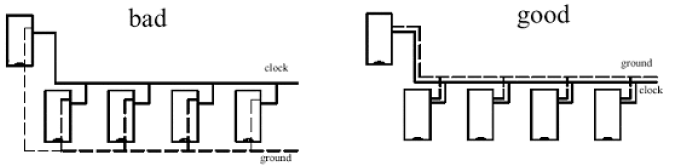
Clock lines are one of the most influential factors on EMC. Avoid vias on clock lines, minimize parallel routing with other signal lines, and keep them away from general signal lines to avoid interference. Also, avoid routing near the power section on the board to prevent interference between power and clock.
If there is a dedicated clock chip on the board, do not route under it; instead, place copper below it and, if necessary, isolate it with ground. For many chips with reference crystal oscillators, do not route under these crystals; use copper for isolation.
2. Right-Angle Routing:
Right-angle routing is generally to be avoided in PCB routing and has become one of the standards for evaluating routing quality. So how much impact does right-angle routing have on signal transmission? In principle, right-angle routing changes the line width of the transmission line, causing impedance discontinuity. Not only right-angle routing but also abrupt angles and sharp angles can cause impedance changes.
The impact of right-angle routing on signals is mainly reflected in three aspects:
First, corners can be equivalent to capacitive loads on the transmission line, slowing down rise times;
Second, impedance discontinuity can cause signal reflection;
Third, right-angle tips can generate EMI.
3. Differential Routing:
Refer to: Altium Designer — Differential Routing and Impedance Matching
Differential signals are increasingly used in high-speed circuit design, and the most critical signals in the circuit often require differential structure design. Definition: Simply put, it means that the driver sends two equal, inverted signals, and the receiver determines the logic state “0” or “1” by comparing the voltage difference between these two signals. The pair of lines carrying differential signals is called differential routing.
The advantages of differential signals compared to ordinary single-ended signal routing are most evident in the following three aspects:
a. Strong anti-interference ability, as the coupling between the two differential lines is good. When external noise interference exists, it is almost simultaneously coupled to both lines, and the receiver only cares about the difference between these two signals, so external common-mode noise can be completely canceled out.
b. Effectively suppress EMI; similarly, because the polarities of the two signals are opposite, the electromagnetic fields they radiate can cancel each other out. The tighter the coupling, the less electromagnetic energy radiated externally.
c. Precise timing positioning; since the switching changes of differential signals occur at the intersection of the two signals, unlike ordinary single-ended signals that rely on high and low threshold voltages for judgment, they are less affected by process and temperature, reducing timing errors, and are also more suitable for low-amplitude signal circuits. The currently popular LVDS (low voltage differential signaling) refers to this small amplitude differential signal technology.
For PCB engineers, the most important concern is how to ensure that the advantages of differential routing are fully realized in actual routing. Anyone who has touched layout will understand the general requirements for differential routing, which are “equal length, equal distance.”
Equal length is to ensure that the two differential signals always maintain opposite polarities, reducing common mode components; equal distance is primarily to ensure that the differential impedance of both is consistent, reducing reflections. The “as close as possible principle” is sometimes also a requirement for differential routing.
4. Serpentine Routing:
Serpentine routing is a frequently used routing method in layouts. Its main purpose is to adjust delay to meet system timing design requirements. Designers should first recognize that serpentine routing can degrade signal quality and change transmission delays, so it should be avoided as much as possible during routing. However, in actual designs, to ensure that signals have sufficient hold time or to reduce timing offsets among signals in the same group, it is often necessary to intentionally route in a serpentine manner.
Points to note:
Pairs of differential signal lines should generally be routed parallel, with as few vias as possible. If vias are necessary, both lines should be routed together to achieve impedance matching.
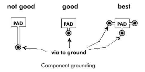
Groups of buses with the same attributes should be routed side by side, achieving equal length as much as possible. Vias leading out from surface mount pads should be as far from the pads as possible.
(3) Common Routing Rules
1. Direction Control Rule for Routing:
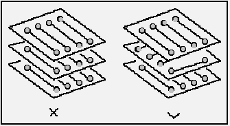
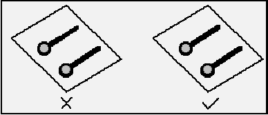
Adjacent layer routing directions should be orthogonal. Avoid routing different signal lines in the same direction on adjacent layers to reduce unnecessary interlayer crosstalk; if this situation is unavoidable due to board structure limitations (such as certain backplanes), especially for high-speed signals, consider using ground planes to isolate each routing layer and isolate each signal line with ground signal lines.
2. Open Loop Check Rule for Routing:
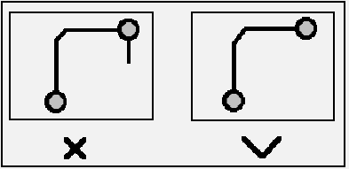
Generally, dangling lines (Dangling Line) are not allowed, primarily to avoid the “antenna effect,” reducing unnecessary interference radiation and reception, otherwise it may bring unpredictable results.
3. Impedance Matching Check Rule:
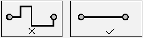
The wiring width of the same network should remain consistent. Changes in line width can cause uneven characteristic impedance of the line, resulting in reflections at high transmission speeds. This situation should be avoided in design. Under certain conditions, such as connector lead wires and BGA package lead wires, changes in line width may be unavoidable, and the effective length of inconsistent sections should be minimized.
4. Length Control Rule for Routing:
This is the short line rule; during design, minimize the routing length to reduce interference issues caused by overly long routing, especially for important signal lines such as clock lines. Ensure the oscillator is placed close to the device. For cases driving multiple devices, determine the network topology structure based on specific conditions.
5. Chamfer Rule:
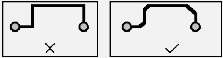
Avoid producing sharp angles and right angles in PCB design to prevent unnecessary radiation and ensure better process performance.
6. Component Decoupling Rule:
A. Add necessary decoupling capacitors on the printed board to filter out interference signals on the power supply, stabilizing the power supply signal. In multilayer boards, the positioning of decoupling capacitors is generally not very high, but for double-sided boards, the layout of decoupling capacitors and the routing method of the power supply will directly affect the stability of the entire system, sometimes even determining the success or failure of the design.
B. In double-sided board design, the current should generally pass through filtering capacitors before being used by devices.
C. In high-speed circuit design, the correct use of decoupling capacitors is crucial for the stability of the entire board.
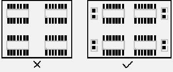
7. Component Layout Partitioning/Layering Rule:
A. This is mainly to prevent mutual interference between modules operating at different frequencies, while minimizing the routing length of high-frequency parts.
B. For mixed circuits, separate analog and digital circuits on different sides of the printed board, using different layers for routing and isolating them with ground layers.
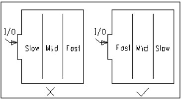
8. Ground Loop Rule:
The minimum loop rule states that the area of the loop formed by the signal line and its return path should be as small as possible. The smaller the loop area, the less radiation emitted externally and the less interference received from the outside.
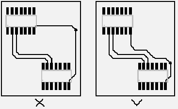
9. Integrity Rule for Power and Ground Layers:
In areas with dense vias, avoid connections between vias in the power and ground layer’s cutout areas, which can disrupt the integrity of the plane layer and increase the loop area of signal lines in the ground layer.
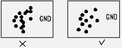
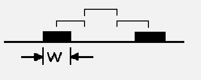
10. 3W Rule:
To reduce crosstalk between lines, ensure that the spacing between lines is sufficiently large. When the center-to-center spacing of lines is no less than 3 times the line width, 70% of the electric field will not interfere with each other, known as the 3W rule. To achieve 98% electric field interference reduction, a 10W spacing can be used.
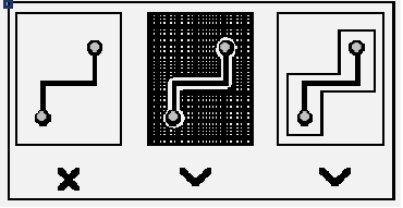
11. Shielding Protection:
Corresponding to the ground loop rule, this is also to minimize the signal loop area, often seen in important signals such as clock signals and synchronous signals. For particularly important and high-frequency signals, consider using a copper shield cable design, isolating the routed line with ground on all sides and effectively integrating the shielding ground with the actual ground plane.
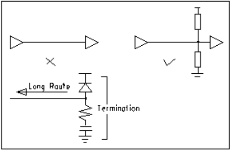
12. Termination Network Rule for Routing:
In high-speed digital circuits, when the delay time of PCB routing exceeds 1/4 of the signal rise time (or fall time), the routing can be considered a transmission line. To ensure the input and output impedance of signals matches the transmission line impedance, various matching methods can be used. The chosen matching method is related to the connection mode of the network and the topological structure of the routing.
A. For point-to-point connections (one output corresponding to one input), series matching at the start or parallel matching at the end can be chosen. The former is simple and cost-effective but has higher delay; the latter has better matching effects but is complex and costly.
B. For point-to-multipoint connections (one output corresponding to multiple outputs), when the network topology is a daisy chain, choose parallel matching at the end. When the network is star-shaped, refer to point-to-point structure. Star and daisy chain are two basic topological structures; other structures can be considered variations of these basic structures, and flexible measures can be taken for matching. In practical operations, consider factors such as cost, power consumption, and performance, generally not pursuing complete matching, but rather limiting interference caused by mismatch reflections to an acceptable range.
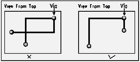
13. Loop Check Rule for Routing:
Prevent signal lines from forming self-loops between different layers. This issue is common in multilayer board designs, and self-loops can cause radiation interference.
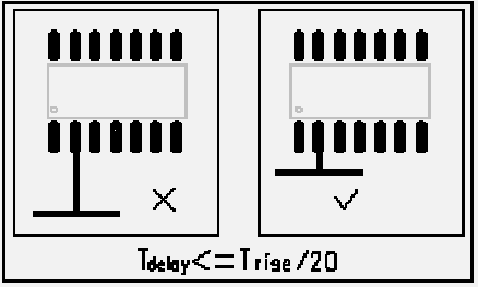
14. Branch Length Control Rule for Routing:
Control the length of branches as much as possible; the general requirement is Tdelay<=Trise/20.
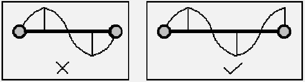
15. Resonance Rule for Routing:
This mainly applies to high-frequency signal design, meaning the routing length should not be an integer multiple of its wavelength to avoid resonance phenomena.
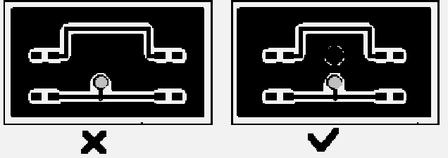
16. Isolated Copper Area Control Rule:
The appearance of isolated copper areas can lead to unpredictable problems, so connecting isolated copper areas with other signals helps improve signal quality, usually by grounding or removing the isolated copper area. In actual manufacturing, PCB manufacturers often add copper foil to some empty parts of the board, primarily for ease of PCB processing and also to help prevent board warping.
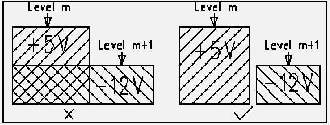
17. Overlapping Power and Ground Layer Rules:
Different power layers should avoid overlapping in space. This is primarily to reduce interference between different power supplies, especially between power supplies with large voltage differences. The issue of overlapping power planes should be avoided, and when unavoidable, consider using a ground layer in between.
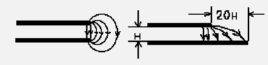
18. 20H Rule:
Due to the changing electric field between power and ground layers, electromagnetic interference radiates outward at the edges of the board, known as edge effects.
The solution is to retract the power layer, ensuring that the electric field only propagates within the ground layer. By retracting 20H (the thickness of the medium between power and ground), 70% of the electric field can be confined within the edge of the ground layer; retracting 100H can confine 98% of the electric field.
(4) Others
For single and double-sided boards, power lines should be as thick and short as possible. The width requirements for power and ground lines can be calculated based on 1mm line width corresponding to a maximum of 1A current, minimizing the loop formed by power and ground.
To prevent coupling noise from entering load devices through long power lines, decouple the power supply before entering each device. Additionally, to prevent mutual interference, independently decouple the power supply for each load and ensure filtering before reaching the load.
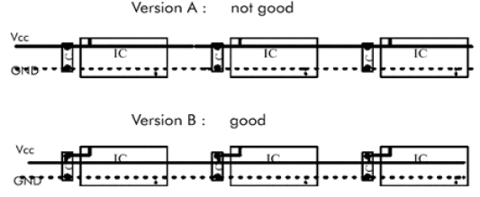
Maintain good grounding during routing. See the diagram below.
3. DDR Routing Rules
(1) First, understand the composition of DDR2 signals:
The DDR2 chip I use is: MT47H64M16HG
Package:
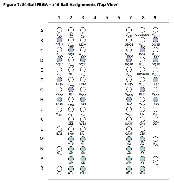
Pin definitions:
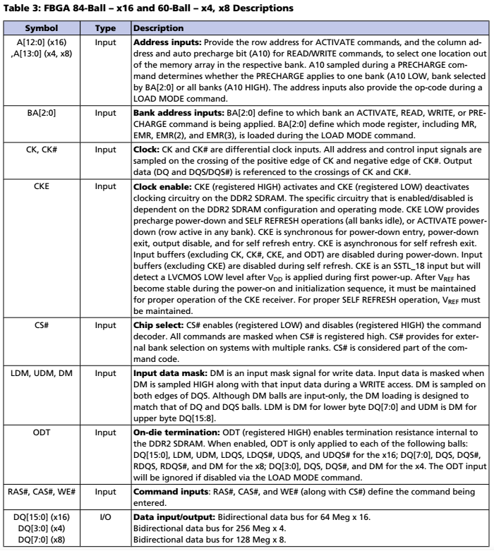
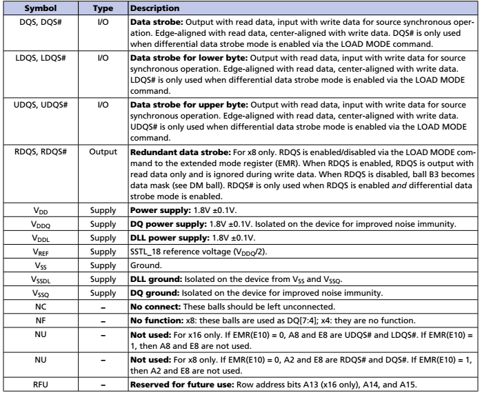
Schematic:
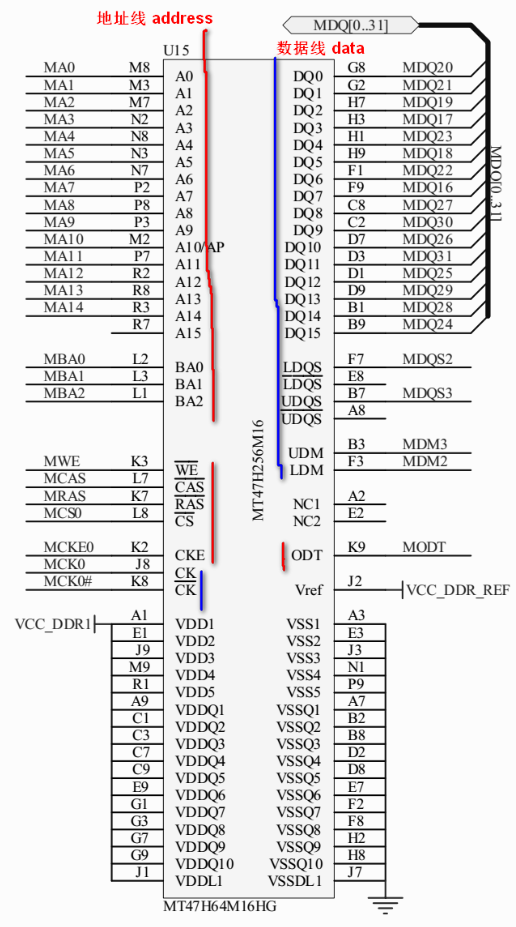
Data lines and address lines:
Data lines: DQ[0-15], DQS, DM, (clock signal) CK/CK#
Address lines: A[0-15], BA[0-2], (control signals) CS/WE/RAS/CAS, CKE, ODT
More Exciting:
Yan Shi│Reflections and Suggestions on the “Dilemma” of Young Teachers in Higher Education
【Directory】”Computer Education” 2022 Issue 9
【Directory】”Computer Education” 2022 Issue 8
【Directory】”Computer Education” 2022 Issue 7
【Directory】”Computer Education” 2022 Issue 6
【Directory】”Computer Education” 2022 Issue 5
【Editorial Message】Professor Li Xiaoming from Peking University: Thoughts from the “Year of Classroom Teaching Improvement”…
Professor Chen Daoxu from Nanjing University: Teaching students to ask questions and teaching students to answer questions, which is more important?
【Yan Shi Series】: Trends in Computer Discipline Development and Their Impact on Computer Education
Professor Li Xiaoming from Peking University: From Interesting Mathematics to Interesting Algorithms to Interesting Programming—A Path for Non-Professional Learners to Experience Computational Thinking?
Reflections on Several Issues in First-Class Computer Discipline Construction
New Engineering and Big Data Major Construction
Lessons from Other Mountains Can Help You—Compilation of Research Articles on Computer Education at Home and Abroad