
「Xilinx Common IP Core Series」
Design and Implementation of a Signal Generator Based on DDS (Includes Verilog Code + Simulation Waveform)
In fields such as communications, radar, and test instruments, the signal generator is one of the most fundamental and important modules. Whether for system validation or algorithm experimentation, a stable and flexible waveform source is essential.
Traditional analog oscillators, while structurally simple, often struggle to meet the demands of modern high-speed digital communications in terms of frequency resolution, switching speed, and flexibility. In contrast, Direct Digital Synthesis (DDS) technology has gradually become the mainstream solution for waveform generation on FPGA platforms due to its high resolution, fast tuning, and phase-controllable advantages.
In Xilinx FPGAs, engineers can not only directly use the official DDS Compiler IP core to quickly complete designs but also implement a custom Verilog HDL to create a DDS signal generator with adjustable frequency to meet the flexible needs of research and education.
This article will guide you through the implementation of a DDS-based FPGA signal generator from four dimensions: Basic Principles of DDS → Vivado Development Environment → Verilog Implementation → ModelSim Simulation Results, providing code and waveform validation to help you quickly get started with this commonly used IP core.
This article focuses on the DDS-based signal generator. The full text is divided into the following four sections:
1. Basic Principles of DDS IP;
2. Development Environment for DDS-based Signal Generators;
3. DDS Signal Generator with Adjustable Frequency (Verilog Implementation);
4. Simulation Test Results Based on ModelSim.


DDS Compiler
1
Basic Principles
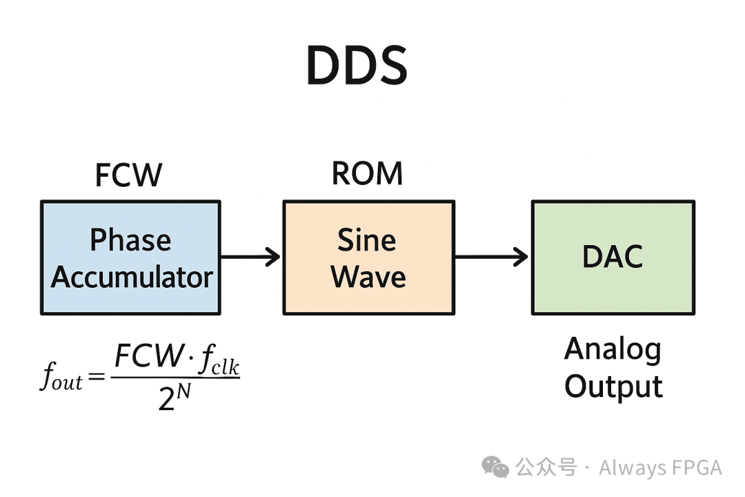
**DDS (Direct Digital Synthesis)** is a digital waveform synthesis technology whose core structure consists of a phase accumulator + waveform lookup table + DAC.
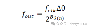
🔹Phase Accumulator: Continuously accumulates phase based on the frequency control word (FCW). The output frequency f_out of the DDS waveform is determined by the system clock frequency f_clk, the phase width in the phase accumulator, and the phase increment. The output frequency (in Hz) is defined as (Formula Source: XILINX IP Core Documentation PG141-dds-compiler-en-us-6.0):
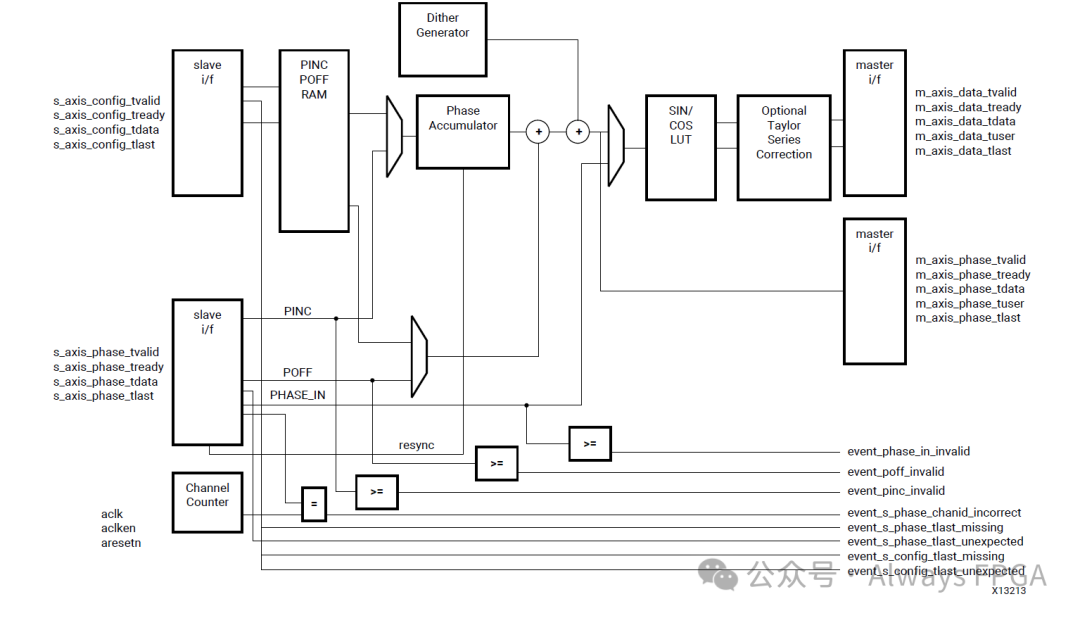
🔹Waveform Lookup Table (ROM/LUT): Maps phase to sine/cosine amplitude values. This core consists of two main parts, the phase generator core SIN/COS LUT, which can be used independently or in conjunction with an optional jitter generator to achieve digital phase-locked loop (DDS) functionality. It supports time-division multiplexing (TDM) multi-channel functionality, where the phase increment core offset parameters can be configured independently. The structural block diagram of the core is shown below (Figure Source: XILINX IP Core Documentation PG141-dds-compiler-en-us-6.0).
🔹DAC Interface: Converts digital waveforms to analog signal outputs. One application scenario of the DDS IP core is that after generating waveforms of corresponding frequencies through DDS in the FPGA, they can be collected and sent through a digital front-end AD/DA, as shown in the figure below.
Advantages:
🔹 Extremely high frequency resolution, reaching sub-Hz levels;
🔹 Can quickly switch frequency and phase, suitable for frequency-hopping communication;
🔹 Fully implementable within the FPGA without additional hardware.
👉Application Scenarios: Frequency-hopping communication, spread spectrum systems, digital modulation, radar signal simulation, etc.
2
Development Environment
In Xilinx FPGAs, the implementation of DDS mainly relies on the Vivado IP Catalog which provides the DDS Compiler IP.
🔹Development Tools: Vivado Design Suite (recommended version 2020.2 and above);
🔹IP Invocation: Search for “DDS Compiler” in the IP Catalog and configure phase width, output width, sampling rate, etc. through the GUI;
🔹Interface Selection: Supports AXI4-Stream or local interfaces;
🔹Testing Environment: ModelSim or Vivado Simulator;
🔹Hardware Platform: ZYNQ-7000 series (e.g., ZYNQ7020-CLG400-2).
🔹Code Text Editor: Microsoft VS Code
🌟 Tip: For beginners, directly invoking the IP core can quickly achieve results; while for research or customization needs, writing Verilog HDL is more flexible.
3
Verilog HDL Implementation
This article will guide you step by step in designing a simple DDS-based signal generator in the PL.
Step 1: Determine the mode of the DDS IP core. There are three modes available for the DDS IP core, each described as follows. This experiment will choose the Phase Generator and SIN/COS LUT (DDS) mode:
Phase Generator: The phase generator consists of an accumulator and an optional adder to allow for phase offset addition. When customizing the core, the phase increment (PINC) and phase offset (POFF) can be independently configured as fixed values, programmable (via configuration channels), or streaming (via the input PHASE channel).
SIN/COS LUT: When configured only as a SIN/COS LUT, the phase generator is not implemented, and the PHASE-IN signal is input through the input PHASE channel and converted to sine and cosine outputs via the lookup table. Efficient memory usage is achieved by utilizing the symmetry of the sine wave. This core can be configured to output only sine waves, only cosine waves, or both (orthogonal) outputs.
Phase Generator and SIN/COS LUT (DDS): The phase generator is used in conjunction with the SIN/COS lookup table to provide a phase-truncated direct digital synthesizer or a Taylor series corrected direct digital synthesizer.
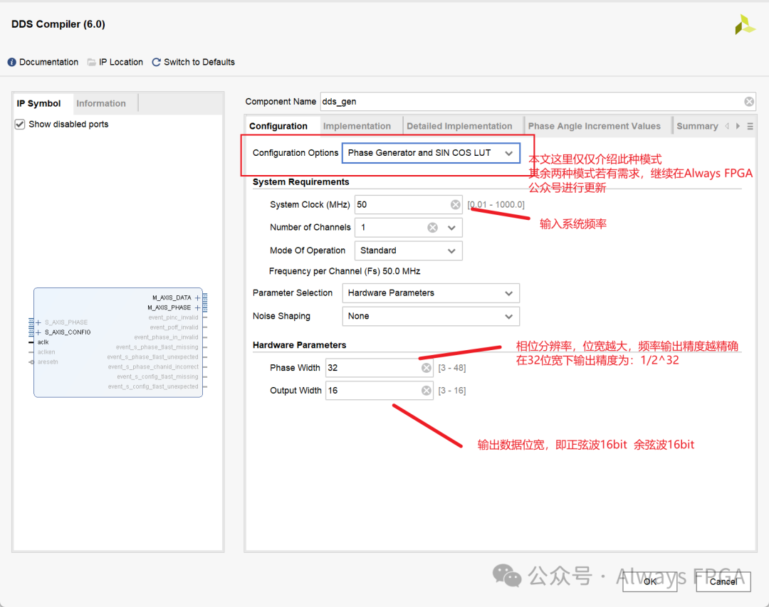
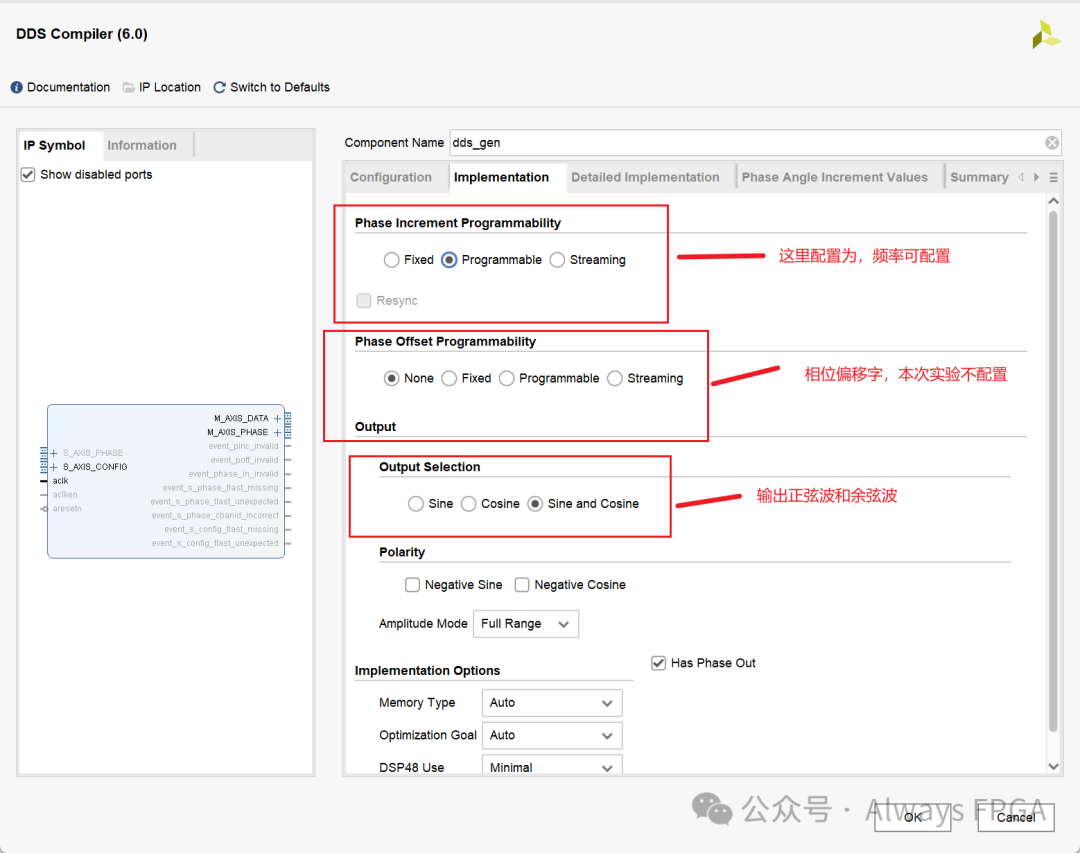
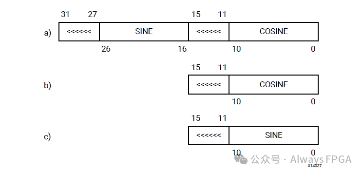
On the subsequent IP core settings page, keep the defaults. It is important to support that the output sine and cosine waves are specified in the previous step, and the positional relationship of the two wave outputs is shown in the figure below (sine wave first, cosine wave second):
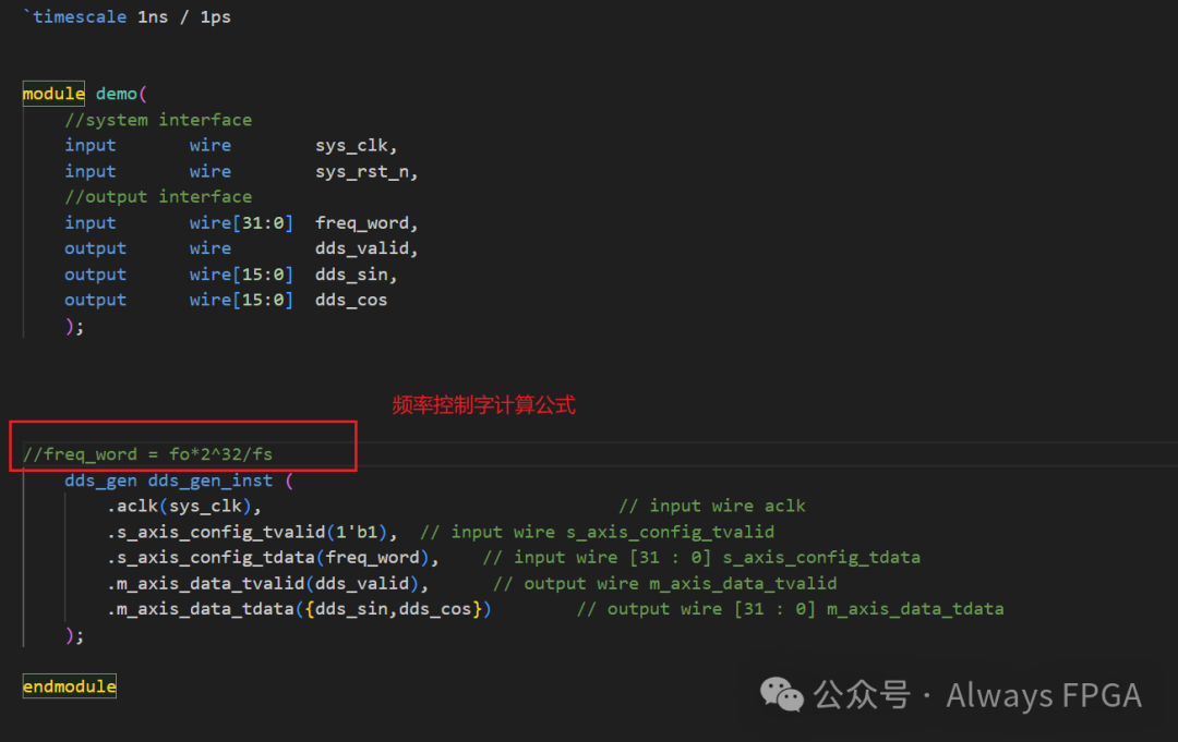
Step 2: Write simple Verilog HDL code. The simple test code written for the PL side is shown in the figure below.
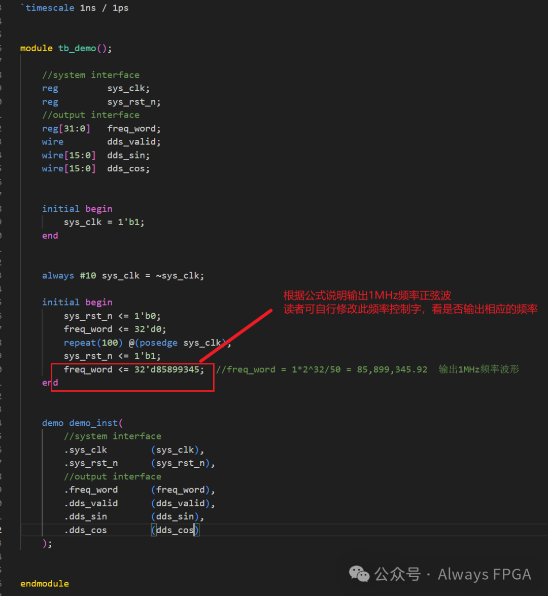
Step 3: Write the corresponding TB file for simulation testing.
4
ModelSim Simulation Test Results
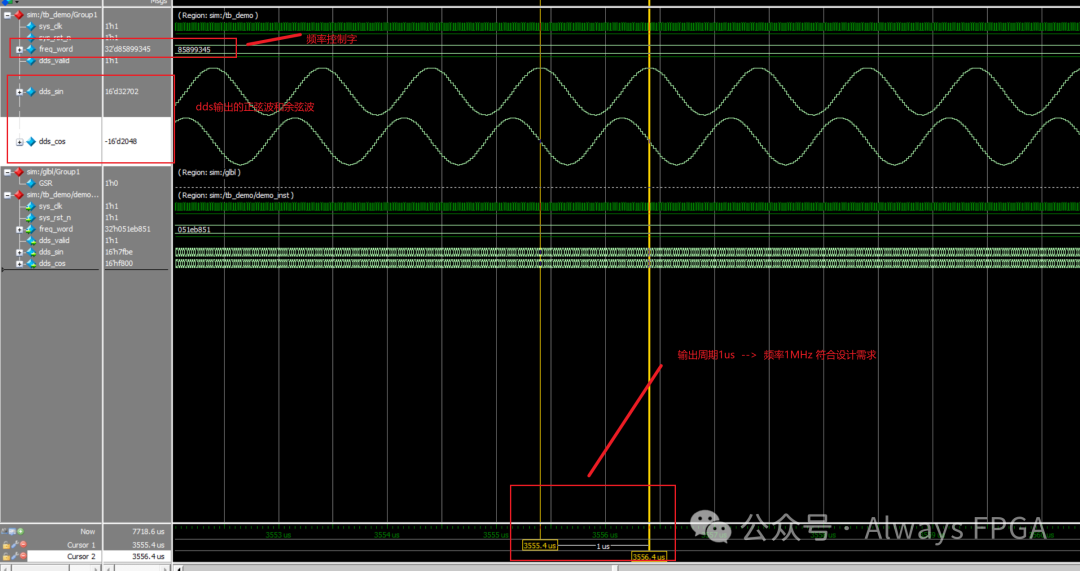
To verify the correctness of DDS, functional simulation was conducted in ModelSim. The simulation waveform shows that the sine wave is smooth and free of glitches; the frequency resolution reaches sub-Hz levels; the ModelSim simulation results are shown in the figure below, with output sine and cosine waves at a frequency of 1MHz, meeting our design requirements.
5
Summary
From principle analysis to HDL implementation and simulation verification, we have completed the design process of a DDS-based signal generator. It can be seen that by utilizing the Xilinx FPGA platform, directly invoking the DDS Compiler IP core can efficiently generate high-precision, dynamically adjustable waveform signals.
In practical engineering, such DDS signal generators can be applied not only in modulation and demodulation, spread spectrum, and frequency hopping in communication systems but are also widely used in radar signal simulation, laboratory testing instruments, and other scenarios. Furthermore, if combined with the AXI4-Lite register interface, dynamic control from the host computer can be achieved, creating a flexible and configurable intelligent signal source system.
As we mentioned at the beginning, the signal generator is an essential tool in FPGA design. Mastering DDS technology not only helps us navigate experiments and validations more smoothly but also lays a solid foundation for future more complex system designs.
This article is the second in the “Xilinx Common IP Core Series”, focusing on the DDS-based signal generator, walking through the process from principle to simulation.
If you feel intrigued, don’t worry—subsequent articles will continue to explore:
🔹 CORDIC-based NCO (Numerically Controlled Oscillator) Design — more storage-efficient compared to DDS;
🔹 DDS Dynamic Control Based on AXI Bus — achieving real-time frequency and phase modulation from the host computer;
🔹 Multi-channel IQ Signal Source Design — aimed at communication applications such as QPSK/OFDM.
👉 Stay tuned!!!

Future Update Plans
Practical explanations of commonly used IP cores;
Practical applications of the AXI protocol, utilizing various operations to experiment with PL-PS data interaction;
FPGA implementation of AD9361 interface transceivers;
Modulation and demodulation of spread spectrum communication and its FPGA implementation;
Modulation and demodulation of OFDM and its FPGA implementation;
If there are any topics you would like to see, feel free to message me, and I will consider updating related content.


This article is an original work by Always FPGA, please indicate the source when reprinting. If you wish to join the group for discussion, feel free to contact me.


End