Where Does the “Speed” of FPGAs Come From?
Among processor families, FPGAs (Field Programmable Gate Arrays) are renowned for their “hardware-level acceleration,” particularly excelling in fields such as high-performance computing, image processing, and communication protocol processing. Their “speed” does not solely rely on clock frequency (many FPGAs operate at only a few hundred MHz, far below the GHz levels of CPUs/GPUs), but rather stems from architectural design, parallelism, and hardware programmability, which are the three core advantages. Below, we will start from the underlying architecture and gradually uncover the secrets of FPGA “speed”.
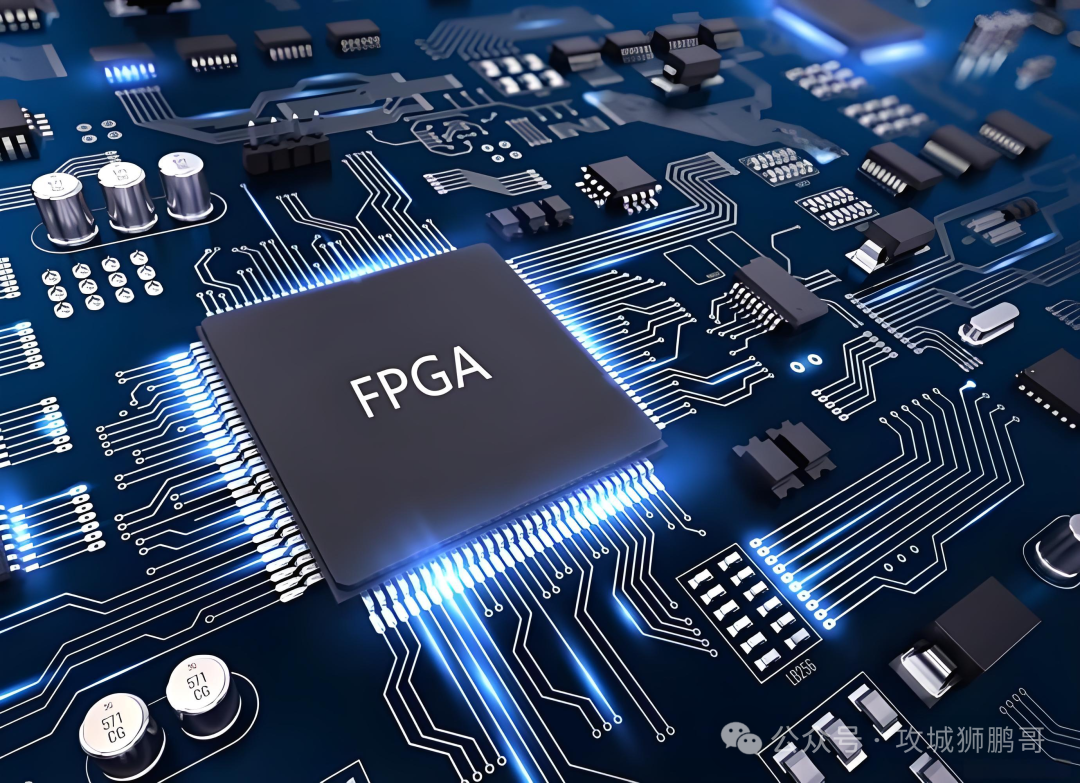
Architectural Layer: A Distributed Hardware Architecture Designed for Parallelism
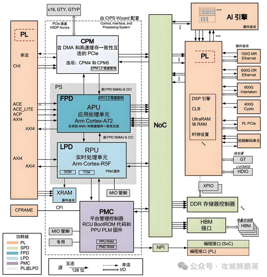
1. Unlike the “Modular” Hardware Structure of CPUs/GPUs
The physical structure of an FPGA resembles a collection of freely combinable “electronic building blocks,” consisting of three main modules:
- Logic Elements (LE/CLB) are the smallest computational units, containing lookup tables (LUTs for logic operations), registers (to store intermediate results), and multiplexers (for data routing). A single FPGA can integrate millions of LEs, equivalent to millions of “micro-processors” working in parallel.
- Interconnect Resources are programmable wiring resources, such as wires and switch matrices, allowing high-speed interconnection between any logic units, with delays that can be precisely controlled (in the nanosecond range).
- I/O Blocks (IOB) support high-speed serial/parallel interfaces (such as DDR, PCIe, SerDes), directly interfacing with external devices to reduce data input/output latency.
This distributed architecture sharply contrasts with the centralized architecture of CPUs, which consists of “core + cache + bus”: CPUs rely on bus scheduling for data, while each logic unit in an FPGA can independently process data and communicate directly “point-to-point” through interconnect resources, avoiding bus congestion and bottlenecks from global controllers.
2. Hardware-Level “Custom Circuits”: Physical Implementation Close to Algorithms
When traditional CPUs execute programs, they must convert algorithms into instruction streams, which are parsed and scheduled for execution by controllers one by one. In contrast, FPGAs can directly map algorithms to dedicated circuits using hardware description languages (Verilog/VHDL). For example:
- To implement a multiplier: a CPU needs to call a multiplication instruction (which may take multiple clock cycles), while an FPGA can instantiate an on-chip dedicated multiplier (DSP Block) directly, completing the computation in one clock cycle.
- To implement data stream processing: for matrix operations in convolutional neural networks, an FPGA can allocate weights and data to thousands of parallel multiply-accumulate units (MACs), computing products at different locations simultaneously without software loop scheduling.
This “hardware as algorithm” characteristic allows the computational flow of FPGAs to be closer to the mathematical essence, reducing overhead from instruction parsing, branch prediction, cache misses, and other software layers.
Parallel Computing Layer: Spatial Parallelism vs. Temporal Parallelism, Extreme Parallel Granularity
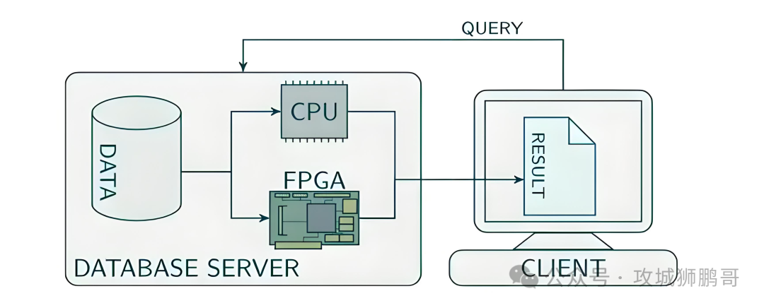
1. Beyond the “Spatial Parallel” Paradigm of CPUs/GPUs
There are two basic modes of parallel computing:
- Temporal Parallelism (CPU/GPU) splits tasks in the time dimension through pipelining (such as a 10-stage instruction pipeline in CPUs) and multithreading (thousands of CUDA cores in GPUs), where each core executes instructions sequentially, relying on clock synchronization for coordination.
- Spatial Parallelism (FPGA) allocates independent computing units for each sub-task at the hardware level, allowing multiple units to operate without clock synchronization (asynchronously), directly processing different data simultaneously. For example:
- To add eight 8-bit data: a CPU needs to loop through 8 addition operations, or use SIMD instructions (Single Instruction Multiple Data) to process them at once; whereas an FPGA can instantiate 8 adders directly, computing simultaneously with a delay equal to that of a single adder (in the nanosecond range).
FPGA’s parallel granularity can be as fine as bit-level (such as processing a single binary bit operation) or data path level (such as independent multiplication and addition pipelines), while the parallel granularity of CPUs/GPUs is at least “instruction level” or “thread level,” with lower flexibility and parallel density.
2. Seamless Integration of Pipelining and Task-Level Parallelism
FPGAs support multi-layer pipelining design:
- Data Pipelining breaks complex computations into multiple stages (such as multiplication → addition → accumulation), with each stage processed by independent logic units, allowing data to flow like an “assembly line,” producing results every clock cycle.
- Task Pipelining allocates independent hardware modules for multiple independent tasks (such as processing multiple frames in a video stream) to work in parallel without operating system scheduling.
For example, when processing high-definition video encoding, an FPGA can simultaneously run video decoding (hardware module A), noise reduction (hardware module B), and encoding (hardware module C), with the three modules working independently, and data flowing directly from A to B to C, with delays only from wiring between modules, rather than the millisecond-level delays of software thread switching.
Hardware Programmability Layer: Tailored Acceleration Strategies
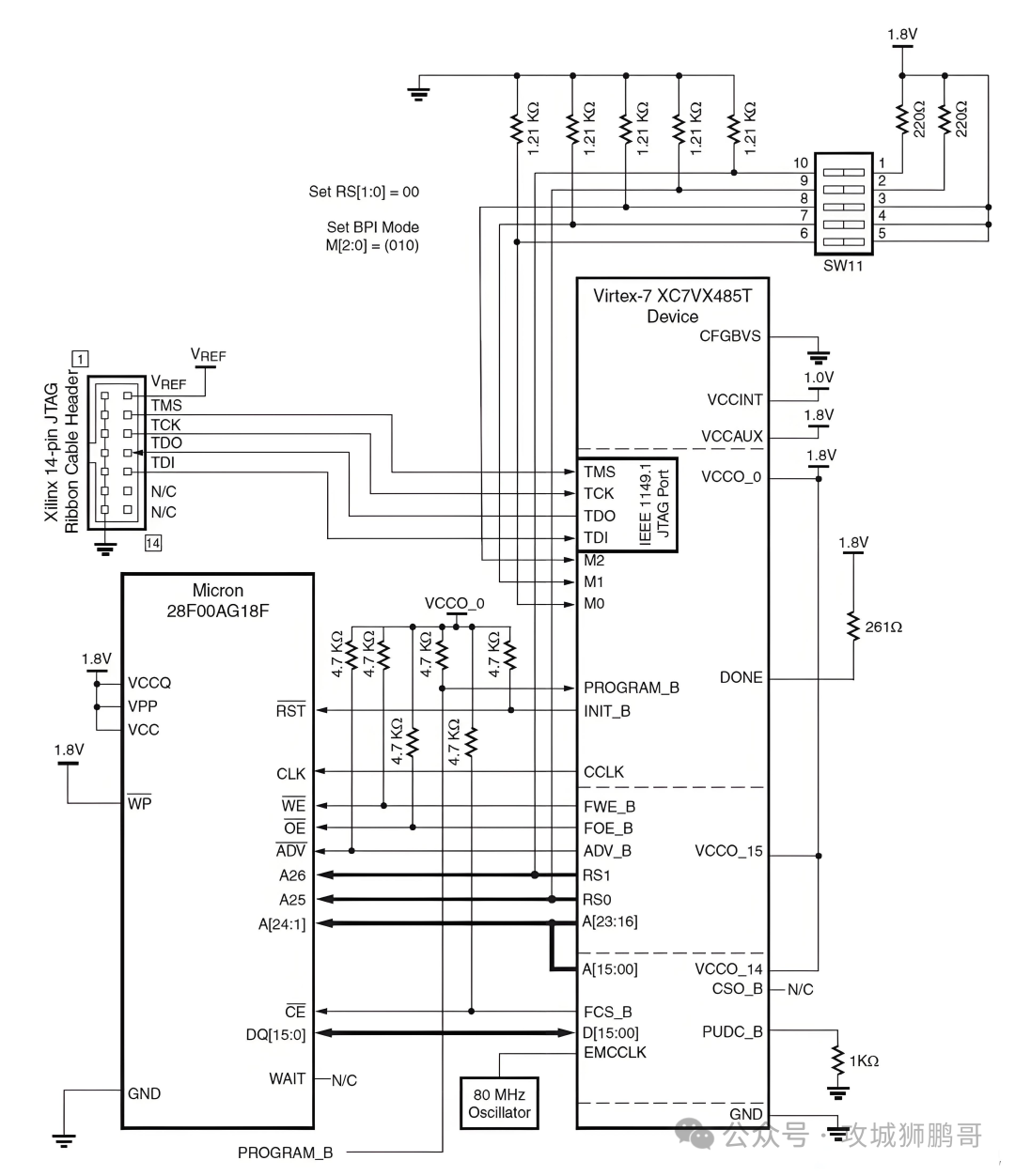
1. Bypassing the Von Neumann Bottleneck: Data Localization and Computation Fusion
Traditional CPUs follow the “Von Neumann architecture”: computation units and storage units are separate, requiring frequent data movement between memory and the CPU. FPGAs reduce data movement through the following methods:
- On-Chip Storage Resources integrate large amounts of BRAM (Block RAM), registers, and distributed RAM, allowing data to be stored close to computation units. For example, when computing matrix multiplication, weights and input data can be preloaded into BRAM, avoiding multiple accesses to external DDR memory (DDR access latency is about 100 nanoseconds, while BRAM access latency is only a few nanoseconds).
- Fusion of Computation and Storage allows logic units to have built-in registers, enabling them to store intermediate results during computation without needing to transfer through a bus. For instance, the output of an adder can be directly connected to the input of a register, participating in the next computation in the next cycle immediately.
2. Eliminating Redundant Operations: Hardware-Level Algorithm Optimization
Even efficient C code executed in software must handle additional overhead from compiler optimizations, instruction alignment, and exception handling. In contrast, FPGAs can directly implement “bare algorithms”:
- Removing Conditional Branches For if-else logic, FPGAs can implement hardware circuits for both branches in parallel, using multiplexers to output results based on conditions, avoiding CPU branch prediction errors (pipeline flushing can lead to delays of dozens of cycles).
- Custom Data Bit Widths allow the use of 8-bit/16-bit/32-bit data paths based on algorithm requirements, rather than the fixed 64-bit registers of CPUs, reducing unnecessary data processing. For example, in image processing, 8-bit pixel data is commonly used, and FPGAs can directly use 8-bit adders, while CPUs must first extend to 64 bits before computation.
3. The “Ultimate Form” of Hardware Acceleration: ASIC-like Performance with Programmability
ASICs (Application-Specific Integrated Circuits) are chips customized for specific tasks, offering extremely high speeds but lacking flexibility. FPGAs can create “virtual” ASIC-like dedicated circuits on the chip through hardware description languages + layout and routing tools:
- Design Process: Users write Verilog code → synthesis tools convert the code into logic unit connection relationships → layout and routing tools map the logic to specific locations on the FPGA chip, optimizing interconnect delays.
- Result: The connections and timing paths of each logic unit are customized for specific algorithms, with almost no redundant circuits, achieving performance close to ASICs (with delays controllable within 5-10ns per operation), while also supporting dynamic reconfiguration (some FPGAs support reconfiguration during operation).
Storage and Data Processing Layer: A “Zero-Copy” Architecture Close to Data
1. Multi-Level Storage Hierarchy Optimization
FPGA storage resources are divided into three layers, with progressively lower latency:
- Off-Chip Storage (DDR/GDDR) has large capacity and high latency (~100ns), connected via high-speed interfaces (such as DDR4-3200).
- On-Chip BRAM/URAM has medium capacity (tens of MB), low latency (~5ns), and supports dual-port simultaneous read/write, suitable for storing intermediate results.
- Registers/Flip-Flops have minimal capacity (each logic unit comes with multiple registers) and extremely short latency (~1ns), used for temporary data storage.
During data processing, FPGAs prioritize storing frequently accessed data in registers or BRAM, reducing reliance on off-chip storage. For instance, weights in convolutional neural networks can be preloaded into BRAM, and input data can flow directly into computation units through stream interfaces (such as AXI-Stream), forming a “data flow processing” mode that avoids the common “memory wall” issues seen in CPUs/GPUs.
2. Dedicated Hardware Modules Accelerating Key Operations
Modern FPGAs integrate a large number of hard IPs, further enhancing the speed of specific tasks:
- DSP Blocks are dedicated multiply-accumulate units that support floating-point/fixed-point operations, completing multiply-accumulate operations in a single clock cycle, with densities reaching tens of thousands per chip (e.g., Xilinx UltraScale+ FPGAs contain over 4000 DSP Blocks).
- Hard Processors (such as ARM Cortex-A) Some FPGAs integrate CPU hard cores for control logic (such as configuring hardware parameters), avoiding excessive complexity in state machines in pure hardware designs.
- High-Speed Interface IPs natively support PCIe, 100G Ethernet, HDMI, etc., allowing data to enter hardware computation modules directly without going through CPU protocol stacks.
Low Latency Design Layer: Fine Control from Timing Optimization to Synchronization Mechanisms
1. Hardware-Level Timing Analysis and Optimization
FPGA development tools (such as Vivado, Quartus) provide precise timing analysis, allowing users to manually optimize critical paths:
- Pipelining Cuts insert registers in long combinational logic paths, distributing delays across multiple clock cycles to improve clock frequency.
- Register Retiming moves registers from one end of a logic path to the other, balancing delays across stages and avoiding overload in a single stage.
- Critical Path Priority Routing allocates dedicated high-speed interconnect resources for high-frequency data paths, reducing signal attenuation and crosstalk.
This “visibility” and “controllability” of hardware timing is something software programming cannot achieve—CPU developers can only optimize indirectly through compilers, while FPGA developers can directly manipulate hardware delays.
2. Flexible Choice of Synchronous and Asynchronous Designs
FPGAs support mixed clock domain designs:
- Synchronous Design is driven by global or regional clocks, ensuring all registers act on the same clock edge, suitable for high-speed pipelines.
- Asynchronous Design coordinates data transfer between modules through handshake signals (such as request/acknowledge), avoiding global clock skew, suitable for low-power or cross-clock domain communication.
In contrast, CPUs rely on global clocks and complex clock synchronization circuits, with clock frequency increases limited by chip area and power consumption, while FPGA’s distributed clock resources allow local modules to operate at higher frequencies (some modules can reach 1GHz, while others operate at hundreds of MHz).
Comparison with Traditional Processors: Where Are the Bottlenecks?
|
Feature |
FPGA |
CPU |
GPU |
|
Parallel Mode |
Spatial Parallelism (Fine Granularity) |
Temporal Parallelism (Instruction/Thread Level) |
Data Parallelism (Thread Level) |
|
Data Localization |
On-Chip Storage Directly Integrated into Computing Units |
Relies on Cache, High Cost of Cache Misses |
Relies on Video Memory, Significant Bandwidth Bottlenecks |
|
Instruction Overhead |
No (Hardware Executes Directly) |
Instruction Parsing, Branch Prediction Overhead |
High Kernel Startup Latency (ms Level) |
|
Latency Control |
Controllable Nanosecond-Level Hardware Paths |
Microsecond Level (Affected by OS Scheduling) |
Microsecond Level (Thread Scheduling Delays) |
|
Applicable Scenarios |
Customized High-Speed Data Stream Processing |
General Computing, Control Intensive Tasks |
Large-Scale Homogeneous Data Parallel Computing |
The core bottleneck of CPUs lies in the separation of storage and computation under the “Von Neumann architecture” and the overhead of instruction scheduling at the software level; while GPUs alleviate some of these issues through large-scale thread parallelism, the synchronization between threads and latency from video memory access remain high. In contrast, FPGAs fundamentally reduce the overhead of data movement and instruction processing by embedding computational logic directly into data paths.
Typical Application Scenarios: How FPGAs Leverage Speed Advantages?
1. High-Speed Data Communication (e.g., 5G Baseband Processing)
- Task Requirements: Real-time processing of OFDM modulation and demodulation, channel coding (such as LDPC/Turbo codes), with data rates reaching Gbps levels.
- FPGA Advantages: Parallel implementation of FFT operations for multiple subcarriers, using dedicated hardware modules to accelerate channel decoding, avoiding the software protocol stack delays of CPUs/GPUs.
2. Deep Learning Inference (e.g., Edge AI)
- Task Requirements: Low-latency processing of image/video data, such as real-time object detection in autonomous driving.
- FPGA Advantages: Fixing neural network weights in on-chip BRAM, using parallel MAC units to accelerate convolution calculations, with input data flowing directly into hardware pipelines through stream interfaces, achieving latencies controllable at the 10μs level (far below the hundreds of μs level of CPUs).
3. Financial High-Frequency Trading
- Task Requirements: Nanosecond-level response speed, processing market data and executing trading strategies.
- FPGA Advantages: Directly parsing network data packets (such as FIX protocol) using hardware logic, parallel computing order matching algorithms, avoiding context switching and interrupt delays from software processing.
Core Logic Mind Map of FPGA “Speed”
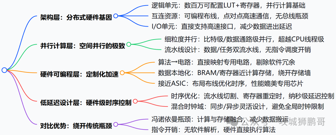
The “Speed” of FPGAs is a Victory of Architecture and Methodology
The “speed” of FPGAs is not due to a single factor, but rather a synergistic result of hardware architecture, parallelism, and programmability. By compiling algorithms into dedicated circuits, data can flow “seamlessly” through customized hardware paths, bypassing the complex software scheduling and storage intermediaries found in traditional processors. This “hardware as algorithm” mindset makes FPGAs irreplaceable in scenarios requiring high-speed data stream processing and customized computing. With the rise of heterogeneous computing, FPGAs are complementing CPUs/GPUs, becoming an important piece in the high-performance computing puzzle.