Welcome FPGA engineers to join the official WeChat technical group.
With the diversification of demand, the functions of FPGAs have been further enhanced. Among them, high-speed transceivers, which were originally modules found only in high-end FPGAs, have become relatively common and even essential functional modules. The 10G line rate has also shifted from being supported by only a few FPGAs years ago to becoming the mainstream line rate today.
The greatest feature of FPGAs is their flexibility, so high-speed transceivers in FPGAs also have very complicated configuration options, aimed at flexibly supporting various transmission protocols. The reason it is considered complicated is that the flexibility brings disadvantages; that is, to clarify many functions, one needs to spend a lot of time on the high-speed transceiver.
However, for most users, the interfaces that require high-speed transceivers are usually relatively fixed, so the functions are also relatively fixed. Therefore, it is unnecessary to understand all the functions of the high-speed transceiver; it is sufficient to understand the meaning of the configurations needed for use. This allows for quick attempts/tests, and during the attempts/tests, a deeper understanding can be combined with the documentation. This might lead to better learning outcomes than forcing oneself to read the entire document before practicing. Therefore, Xilinx’s high-speed transceivers come with default configurations for some commonly used interfaces to facilitate users’ learning/use.
Xilinx 7 series FPGA chips configure four types of high-speed transceivers, ordered from low to high based on the supported maximum line rate: GTP, GTX, GTH, and GTZ. GTP has relatively poor flexibility due to structural issues, and the maximum supported line rate is only 6.x G. GTZ is the highest-end high-speed transceiver in the 7 series, and FPGAs integrating GTZ are rare. It also uses multi-die technology, physically separating it from the FPGA core. This article will not elaborate further on these two GTs. Compared to GTX, GTH has an almost identical overall structure, with only a few more configurations or more powerful performance in specific details. Considering that the documentation is the same, this article takes GTX as an example. All content in this article, unless otherwise specified, applies to both GTX and GTH.
For the high-speed transceiver GTX, although one can initially learn through the default configuration in the IP, and after gaining some foundation, manually configure GTX parameters, the most common issue that arises from insufficient understanding of GTX’s various functions is the inability/not knowing how to correctly locate problems. Therefore, the theme of this text is to introduce some common debugging methods and steps to help users initially locate issues. Even if problem localization is not possible, keeping detailed records of these debugging efforts and submitting them to FAE will also be very helpful.
It should be noted that GTX issues are usually not simple, and debugging work is particularly tedious. Moreover, it may often be in vain, ultimately requiring assistance from FAE/technical support. However, this does not mean that all work can be pushed onto FAE/technical support. Conducting some preliminary debugging and providing feedback to FAE/technical support can help experts understand the problem phenomena more quickly and provide further suggestions without having to start checking from the most basic tasks.
The first step is to generate the GTX example design based on the configured GTX IP and perform simulation.
First, one of the advantages of the Vivado tool is that almost all IPs provide an example design based on IP configuration. For complex IPs like GTX, this example design is a complete project that offers various purposes and is a very useful learning/debugging tool. The first step is to use this project for simulation, which helps understand the specific operations of GTX and compare them with actual results.
It is emphasized that this is not specific to GTX; for any FPGA design, it is recommended to conduct sufficient simulation whenever possible.
The second step is to directly use the GTX example design as the project and check the rx fsm reset done and rx status state machine. If conditions permit, testing with 8b10b in a real environment is advisable.
Let’s explain the role of 8b10b. The role of 8b10b here is to check for 8b10b errors. If 8b10b errors occur, it indicates a high probability of hardware issues, warranting a closer look at PCB routing quality, clock/power, etc. If the 8b10b environment cannot be used (not even in the testing environment), the problem may be more challenging.
The rx fsm reset done is a marker indicating the completion of the receiving end task. Typically, when this signal is high, it indicates no issues at the receiving end, usually meaning that GTX can operate normally. If it cannot be held high stably, one should examine the changes in rx status to see which step (or steps) prevent rx fsm reset done from being held high.
Regarding the sources of these two signals, the example design provides a reset state machine. By default, it is not included in the IP Core but is found in the example design. For the final design, it is recommended to use the example design as a whole rather than just the IP Core.
The third step is to use the ibert tool to test the bit error rate and check the eye diagram.
If the example design can operate normally, unless there are issues with the GTX IP settings, the most basic applications of GTX should generally be fine. If there are issues in the example design testing, where the rx fsm reset done signal cannot be held high and there are 8b10b errors, the next step is to use ibert to check the hardware circuit.
Under conditions where the other end can send prbs (such as when ibert is also running on the other end FPGA), ibert can test the bit error rate. The bit error rate can help check whether there are issues with the link quality.
Regardless of whether the bit error rate test can be conducted, ibert can scan the eye diagram at the receiving end. By observing the size of the eye diagram, one can initially judge the quality of the link.
ibert is a testing tool provided by Xilinx for high-speed transceivers in FPGAs. Typically, after the PCB is completed, ibert can be used to test the link quality of the high-speed transceiver. Additionally, if high and low-temperature testing is required, using ibert is also a good choice.
The fourth step is to conduct external loopback testing when conditions allow.
When FPGAs use high-speed transceivers, a common scenario involves using external cables, such as optical modules/fibers or coaxial cables. In this case, external loopback testing can be performed. The example design can be subjected to external loopback testing, where the signal sent out by the GTX TX is returned to its RX end via external cabling. If this test result is stable, it indicates that GTX can operate normally.
Moreover, there are many situations where external loopback testing is not possible, such as when the transceiver routing is fixed on the PCB, like in PCIe. In such cases, if two Xilinx FPGAs are interfacing, one can consider using the internal far-end loopback of the FPGA for testing. The specific principle is that the TX of the GTX to be tested sends data to the auxiliary FPGA’s GTX, and the auxiliary GTX directly sends the data received from RX back to TX. The RX end of the tested GTX receives the data sent from the TX end of the auxiliary GTX, completing the loopback. This effectively uses the auxiliary GTX to achieve external loopback. It should be noted that the use of far-end loopback is subject to certain conditions; please refer to the 7 series GTX/GTH manual UG476 for specifics.
If the results of the example design are not ideal during external loopback testing, one can use ibert to conduct another test, checking the bit error rate and eye diagram when conditions allow. This can serve as comparative analysis data.
The fifth step is to use a high-speed oscilloscope to check the eye diagram on the RX receiving end PIN of the FPGA GTX, if conditions permit.
This step has the greatest conditional limitations. High-speed oscilloscopes are expensive and complex to use. Additionally, since FPGAs are often BGA packaged, the RX PIN of GTX may not be accessible for testing with oscilloscope probes. Therefore, many users may not be able to conduct this test.
As for the use of the 2D eye scan within GT, theoretically, it can assist debugging. However, in practice, when users can utilize the 2D eye scan, they usually do not need the preliminary debugging suggestions provided in this article. Therefore, this article targets beginner users and does not cover the relatively advanced/complex 2D eye scan.
Next, let’s further analyze the specific roles of steps two to five.
The rx fsm reset done signal in the second step can serve as an indicator signal for the normal operation of GTX. If the example design can stably operate in the final usage/testing scenario, this signal being stable high indicates that the design is almost without issues. If the user’s design encounters problems, it is likely due to issues with the integration of the GTX code, such as not properly using the example design or that the problem does not originate from the GTX module. Additionally, if there are inappropriate configurations, one can refer to simulation and the tests in the fourth step.
It is important to note that the example design uses self-contained data sources and receiving data for comparative validation to determine data accuracy. If users use their own data sources, it may lead to the data validation module continuously outputting errors, causing the rx reset state machine to be perpetually reset.
This issue can be judged by observing the rx status. Other possibilities will also reflect in the changes of the rx status signal. Thus, rx status is a very important debugging signal.
As for 8b10b, its greatest advantage is its built-in error checking. If 8b10b errors occur, it indicates a high probability of link issues.
Building on the second step, testing with ibert is advisable because, in addition to testing the bit error rate and eye diagram (which can also be implemented through custom design logic), ibert pulls out all parameters of GTX for arbitrary configuration. If the findings from the first step suspect hardware link issues, using ibert to check the link is a good approach and allows for adjustments of some GTX parameters to attempt to reduce the bit error rate and enlarge the eye diagram. Additionally, the size of the eye diagram is also of reference significance.
It should be noted that ibert and the GTX example design are completely different designs. Ibret is solely for testing convenience, and many parameter values of GTX differ from those used in actual applications. Thus, compared to ibert, the GTX example design is closer to the final implementation results.
When it is said that there is a high probability of hardware link issues, this conclusion may not be very helpful for debugging. Therefore, loopback testing is necessary. If external loopback testing can be performed and the test results are normal, it may indicate that there is an issue with one end of the termination, or that there is a significant frequency offset in the reference clock of both GTX. If external loopback testing cannot pass, one can enable the near-end PMA loopback for testing (do not use the near-end PCS loopback). If the near-end PMA loopback test is normal, it can be concluded that there are issues with the external link quality (such as problems with the optical module/fiber). If the near-end PMA loopback test does not pass, it is likely that there are issues with the clock/power.
Loopback testing can be conducted twice, once using the GTX example design and once using ibert, to compare results. Causes such as optical fiber issues can yield the same results in both tests. If the results meet expectations, one is closer to identifying the true cause of the problem.
Measuring the eye diagram is the final basis for judging link quality. By using an external oscilloscope and ibert to measure the eye diagram, specific data can be submitted to FAE to determine whether it meets GTX requirements (the manufacturer should have relevant data, but it seems not to be made available for ordinary users to view).
The eye diagrams measured by the oscilloscope and ibert are different. Typically, when using an oscilloscope, the eye diagram measured from the FPGA GTX RX pin is referred to as the far-end eye diagram, while the eye diagram measured by ibert is referred to as the near-end eye diagram.
The far-end and near-end eye diagrams are distinguished based on whether the signal has passed through the RX PMA. The far-end eye diagram is the signal that has not passed through the RX PMA, while the near-end eye diagram is the signal that has been processed by the RX PMA.
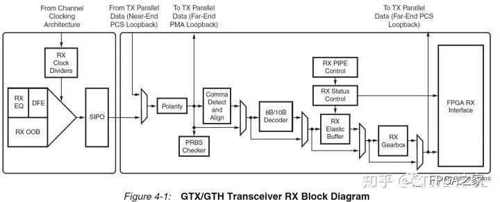
The RX PMA processes the received signal, which has certain processing functions (as shown in the above figure: RX EQ, DFE). The quality of the processed signal improves. Therefore, signals processed through the RX PMA typically have better quality than those at the pin, resulting in the near-end eye diagram being superior to the far-end eye diagram.
Although the specific debugging steps are summarized into five steps, if one is not familiar with them, implementation can still be quite cumbersome. However, since GTX issues are usually relatively difficult to locate, these tests are valuable for reference and enhance understanding of GTX. Conducting relevant tests in advance during the R&D process can help eliminate many problems and facilitate the project proceeding as planned.

Welcome communication engineers and FPGA engineers to follow our public account.

FPGA WeChat technical group
We welcome everyone to join the national FPGA WeChat technical group, where a group of engineers passionate about technology can exchange and discuss technology together!

Press and hold to join the national FPGA technical group.
FPGA IP Core Services: Various high-quality IP core service providers with guaranteed service! If you have needs, you can contact the group owner directly!
FPGA technical group self-operated platform:Xilinx Altera Micron, Samsung, Hynix, ADI TI ST NXP and other brand advantage distributors, feel free to send a model list whenever you have needs, and we will provide you with the most competitive quotes in the first instance!Prices lower than your original suppliers by more than 5%! Welcome to inquire – just send your needs to the group owner!
Official acknowledgment of FPGA technical group brands: Xilinx, intel (Altera), microsemi (Actel), LattIC e, Vantis, Quicklogic, Lucent, etc.