Introduction
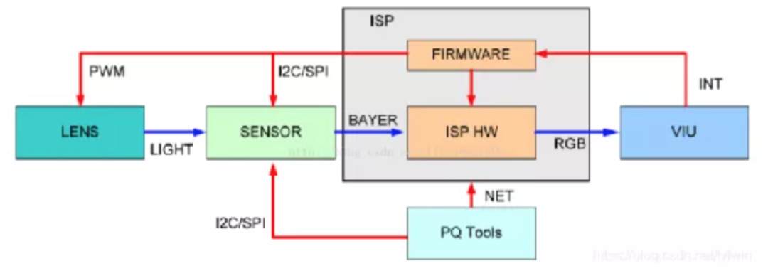
FPGAs are widely used in various image processing applications, including medical and scientific imaging, space imaging, automotive, and defense fields.
No matter which solution is used, the advanced algorithms may differ, but the fundamental parts are the same: they all need to connect to an image sensor or camera, process the captured images, and then organize them into a video stream for display or transmission over a network.
In this project, we will take a detailed look at the different stages and elements involved when using an image sensor.
We will start from the beginning: how does an image sensor actually work?
How Does an Image Sensor Work?
An image sensor is a remarkable device because it allows us to see things not only within the visible spectrum but also beyond, such as X-rays and infrared light.
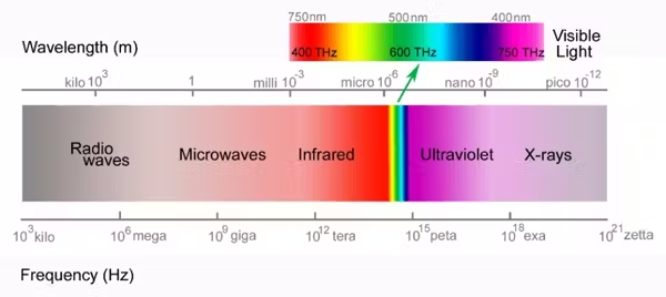
Image sensors are primarily based on two technologies:
- Charge-Coupled Device (CCD)
- CMOS Image Sensor (CIS)
Both work by converting photons striking the semiconductor into voltage.
Charge-Coupled Device – Utilizes potential wells to form a pixel array, with potential wells forming when incident photons strike the pixels. During the integration time (i.e., the time to capture the image), the charge generated by the photons striking the pixels accumulates, like water filling a bucket, until the potential well is full. At the end of the integration time, the charge is output pixel by pixel, converting it to voltage.
This operation is similar to a shift register: a timing signal shifts the stored signal through the pixel array. To speed up the readout, multiple output channels can be implemented. CCDs are analog, and the timing of the signals and voltage levels affect data transmission and the overall quality of the image. Typically, an external ADC is used to convert the pixel voltages into digital representations for further processing.
CCDs are less common today, but they are still used in high-end imaging applications such as astronomy and space imaging due to their superior performance.
CMOS Image Sensor – CIS uses photodiodes to form a pixel array, converting photons into voltage at each pixel. This analog voltage is directly converted to a digital output on the chip.
This conversion method is faster than CCD readout, but CIS typically has poorer noise performance. Most cameras today use CIS because they are easier to operate and integrate digitally.
Imaging Beyond the Visible Spectrum
If we want to image beyond the visible spectrum, we must choose the appropriate equipment. Both CMOS and CCD sensors can capture X-rays to near-infrared (NIR) wavelengths.
As the wavelength decreases towards the infrared spectrum, the energy of the electrons also decreases, requiring more advanced semiconductors than silicon. Depending on the observed spectrum, typical devices include:
- Charge-Coupled Device (CCD): X-rays to visible light, extending into near-infrared.
- CMOS Image Sensor (CIS): X-rays to visible light, extending into near-infrared.
- Uncooled Infrared: Microbolometers, typically operating in the mid-infrared range.
- Cooled Infrared: Solutions based on HgCdTe or InSb that require cooling.
Line Scan or 2D Scan
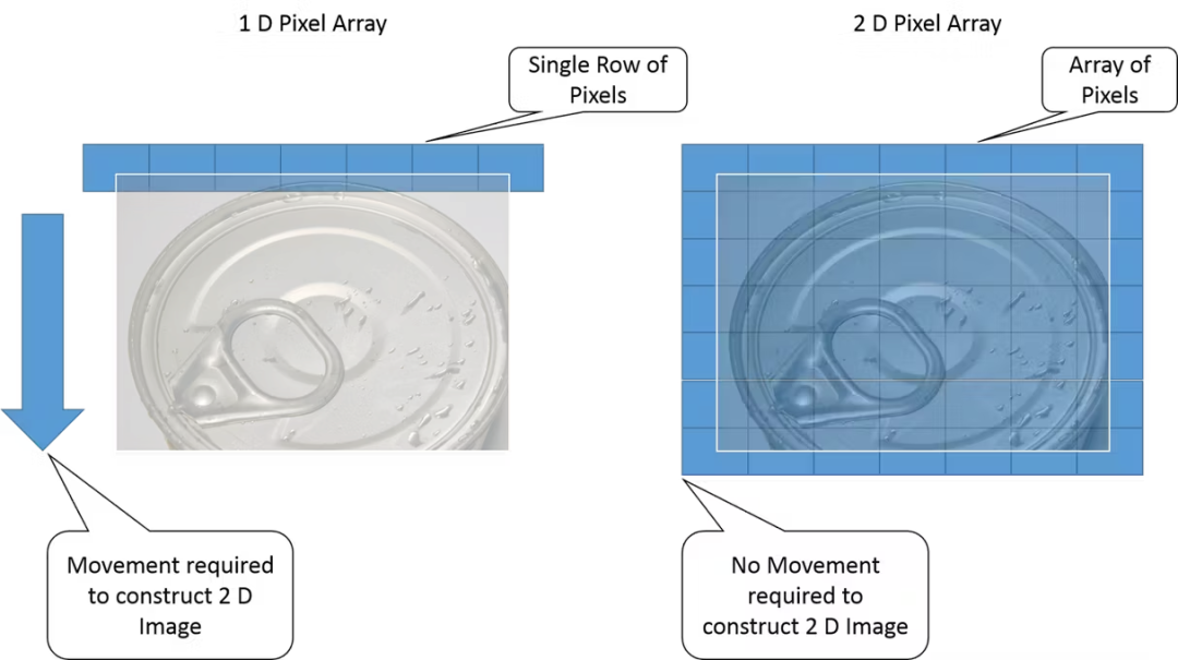
When we view a still image or video frame, it is two-dimensional. However, how a two-dimensional image is created depends on the specific application.
For example, if the target object is moving (such as on a production line), a single line of pixels can be used to generate a two-dimensional image through movement. This method is common in production line inspection and orbital satellite imaging, as the motion of the orbit provides the necessary movement to generate the image.
A more common alternative is to use a 2D sensor that captures 2D images without movement.
Sensor Performance
A key performance metric for image sensors is Quantum Efficiency (QE). QE measures the ratio of the number of photons incident on the device to the number of photons detected in the pixel.
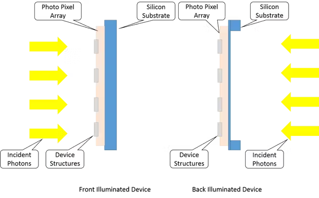
When manufacturing image sensors, the structures on the device can reduce the QE in front-illuminated designs (i.e., where photons strike the front of the sensor).
To achieve better Quantum Efficiency (QE), back-illuminated designs have been adopted to minimize the impact of structures on photon detection. However, back-illuminated designs require additional processing, which can reduce yield and increase costs.
Rolling Shutter or Global Shutter
When using 2D image sensors, we often need to determine the type of shutter on the image sensor. There are mainly two types of shutters:
-
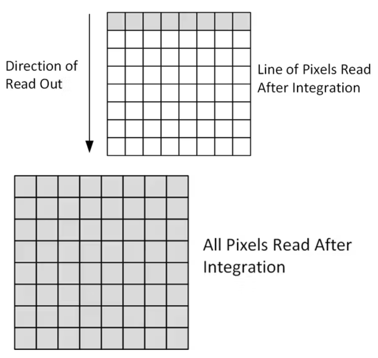
Rolling Shutter: Each row is read out after its integration time, but the captured image may be distorted due to motion.
-
Global Shutter: The entire array is synchronized and read out as a whole.
I believe we have all seen videos online where a helicopter is flying, but the rotor blades appear to be stationary. This is because the rolling shutter is synchronized with the rotor blades, causing them to appear motionless.

Color or Grayscale
For most people, the way we perceive the world through our eyes is in color. However, so far, we have only discussed pixels, the accumulation of charge, and the process of converting charge to voltage and then to digital format.
All wavelengths of photons mix on a pixel and are converted into voltage that represents the image. If we process this information as is in an image processing application, the result will be a grayscale image.
Grayscale images are used in many applications because they provide brightness information, which is crucial for analyzing brightness, contrast, edges, shapes, contours, textures, perspective, and shadows.
Grayscale operations also have the advantage of high computational efficiency, as only a single channel of data needs to be processed. Additionally, using threshold processing makes it easy to convert grayscale images into binary images for morphological operations.
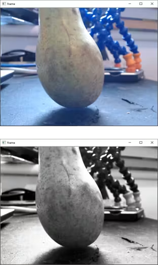
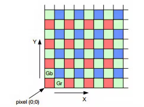
To obtain a color image, a specific optical filter must be applied directly to the sensor. This filter is known as a Bayer mask, which covers each pixel and only allows one wavelength of light (red, green, or blue) to pass through.
Each pixel captures only red, green, or blue photons. These filters are typically arranged in a 2×2 grid, containing one red pixel, one blue pixel, and two green pixels. This arrangement emphasizes green because it is in the middle of the visible spectrum, and the human eye is more sensitive to green light.
Debayering Process
The Bayer mask requires post-processing to reconstruct the full-color image. In an FPGA, we can process the pixel stream and perform debayering on the raw data, using the 2×2 grid to convert each pixel into RGB values.
This process involves interpolation between adjacent pixels in the grid. While effective, it may result in a slight loss of image resolution due to the need for interpolation to fill in the missing color information.
Color Space
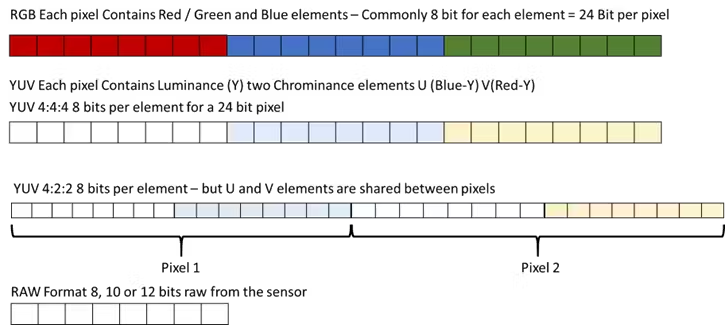
If we decide to process RGB images, we also need to consider the color space. Typically, we start with the RGB color space. Assuming each color channel (R, G, B) is 8 bits, each pixel requires 24 bits.
In an FPGA, any bus size can be easily implemented. However, due to the 24-bit format, storing this data in memory (such as DDR3 or DDR4) is not efficient.
To improve memory efficiency, we can use a more compact color space, such as YUV, which separates the luminance (Y) and chrominance (U and V) channels. In the YUV color space, two pixels can share the U and V channels, reducing the storage requirement to 16 bits per pixel, thus improving efficiency.
Additionally, a narrower bus width simplifies routing within the FPGA, making implementation easier and potentially more cost-effective.
Interfacing with Sensors and Cameras
Now that we understand how image sensors work, we can explore how sensors connect to FPGAs.
There are mainly two methods:
- Camera Integrated Sensors: The sensor is embedded in a camera that performs most of the interfacing and outputs images for further processing.
- Direct Sensor Interface: The FPGA interfaces directly with the sensor, requiring additional control and signal processing.
Regardless of the method used, FPGA I/O is versatile and capable of connecting to cameras and sensors.
Let’s first look at some common interface standards:
- HDMI (High-Definition Multimedia Interface) – HDMI is commonly used for cameras, especially compact action cameras. FPGAs can directly interface with HDMI using the minimized transmission differential signaling (TMDS) standard. AMD 7 series FPGAs, UltraScale™ devices, and UltraScale+™ devices all support this functionality.
For higher resolution images, performance may exceed that of HD storage, and gigabit transceivers can be used. HDMI transmits video data through three differential channels (for red, green, and blue) and an additional channel for the clock signal.
- SDI (Serial Digital Interface) Video – SDI is a professional standard for transmitting uncompressed digital video, audio, and metadata over coaxial cables with BNC connectors or fiber optics.
Supported resolutions: Ranging from standard definition (SD-SDI) to ultra-high definition (12G-SDI).
Applications: Due to its high quality, low latency performance, and support for long cable runs, it is ideal for broadcasting and live production.
FPGA Support: When connected to AMD FPGAs or SoCs, SDI uses gigabit transceivers.
SDI video signals are processed through dedicated hardware IP cores, providing:
Support for various SDI standards. Functions such as video scaling, color space conversion, and multiplexing.
These cores enable powerful and flexible integration with professional video workflows.
- Camera Link – Camera Link uses multiple LVDS (Low Voltage Differential Signaling) channels to transmit data from the camera to the frame grabber (in the Camera Link standard, the frame grabber is our FPGA). Camera Link uses four pairs of LVDS lines to transmit data, with a fifth pair of LVDS lines transmitting the clock.
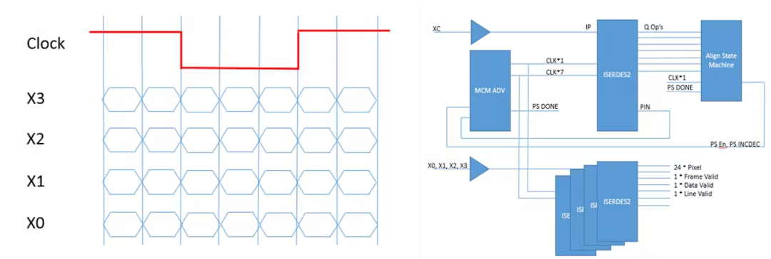
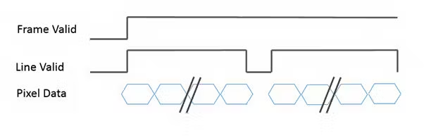
- Parallel/Serial – Many cameras or sensors provide parallel or serial outputs, which can be reconstructed into pixel data, associated frames, and line valid signals through deserialization. This can be implemented using LVDS/SLVS (Scalable Low Voltage Signaling). If serialization is used, the I/O structure provided by the FPGA can be used to synchronize and correctly decode the data stream.
- MIPI (Mobile Industry Processor Interface) – MIPI is one of the most widely used sensor interfaces. It is a high-bandwidth, point-to-point protocol designed to transmit image sensor or display data over multiple differential serial channels.
Protocol Layer: MIPI operates across various OSI model layers, with the lowest being the DPHY layer.
DPHY defines the number of channels, clock, and the conversion between differential signals (SLVS) and single-ended signals (LVCMOS).
This combination supports high-bandwidth data transmission for protocols such as CSI-2 (Camera Serial Interface) and DSI (Display Serial Interface).
Low-speed communication allows for effective transmission of control information at lower power levels.
Performance:
Each MIPI DPHY link can support 1 to 4 high-speed serial channels, with each channel running at speeds up to 2.5 Gbps, or four channels running at speeds up to 10 Gbps.
Data transmission occurs at double data rates, synchronized with the clock channel.
FPGA Support:
AMD UltraScale+ devices and Versal™ Adaptive SoCs natively support MIPI DPHY.
For AMD 7 series FPGAs and UltraScale devices, MIPI DPHY can be implemented using external resistor networks or custom DPHY circuits.
Utilizing Programmable Logic and IP Libraries
The core idea of FPGAs is to leverage as much existing IP (Intellectual Property) from the Vivado™ Design Suite and Vitis™ platform IP libraries as possible. These libraries provide a wealth of pre-designed components that can efficiently implement complex functionalities.
AXI Stream for Video Transmission
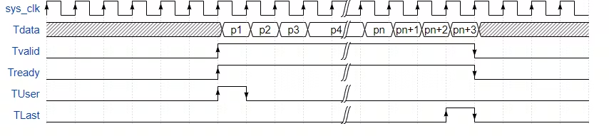
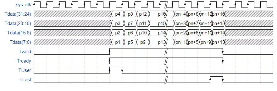
Most interfaces in video processing pipelines use the AXI Stream protocol to transfer video streams between modules. The core operations of AXI Stream primarily use the following signals:
- TData: Transfers the data payload from the master to the slave.
- TValid: Indicates that there is valid data on the TData bus.
- TReady: A signal from the slave device indicating it is ready to accept data.
Video Data Marking
For video streams, additional markers are needed to indicate the start of frames and the end of lines so that complete 2D images can be constructed and processed.
To achieve this, AXI Stream introduces:
- TUse signal: Indicates the start of a new frame.
- TLast signal: Marks the end of a line in the video stream.
These markers ensure the correct synchronization and reconstruction of video data, making the AXI Stream protocol very suitable for handling 2D images and video processing in FPGAs.
Having understood the concept of AXI Stream and its application in image processing stream transmission, we can now explore how to leverage the parallel characteristics of FPGAs. One effective method is to include multiple pixels in a single AXI Stream data flow.
By transmitting multiple pixels per clock cycle, the throughput of the image processing pipeline can be significantly increased.
Leveraging FPGA Parallelism in AXI Stream
<spanhaving a="" and="" application="" axi="" can="" characteristics="" concept="" data="" effective="" explore="" flow.
By transmitting multiple pixels per clock cycle, the throughput of the image processing pipeline can be significantly increased.
Pixel Parallelism in AXI Stream
Typically, AXI Stream can be configured to transmit 1, 2, or 4 pixels per clock cycle, depending on the application and system requirements. For example, when outputting 4 pixels per clock cycle, the overall data rate and processing efficiency will significantly improve, as shown in the following example.
This parallelism not only enhances the performance of FPGA-based image processing pipelines but also ensures seamless processing of high-resolution and high-frame-rate video streams.
FPGA Image Processing Pipeline Architecture
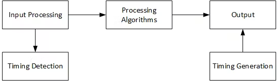
When implementing an image processing pipeline in programmable logic, two main architectures need to be considered:
1. Direct Architecture
In a direct architecture, the input is directly connected to the processing stages and output, with minimal buffering and no frame buffering.
-
Advantages: This approach provides the lowest latency between input and output, making it ideal for applications where latency is critical, such as autonomous vehicles or real-time video analysis.
-
Limitations: Due to the lack of frame buffering, this architecture is less flexible for tasks that require temporal data storage or synchronization.
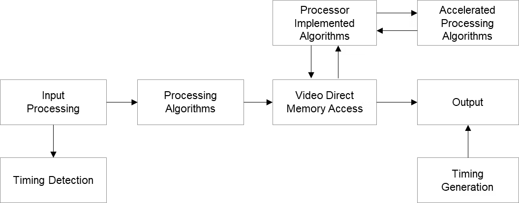
2. Frame Buffer Architecture
The frame buffer architecture utilizes memory to buffer one or more frames.
Advantages: This method is used when:
It is necessary to provide the image to the processing system’s processor.
It is necessary to modify the output timing of the video stream (for example, for synchronization or compatibility with other components).
Use Case: Frame buffer architecture is common in applications where flexibility and timing adjustments are more important than latency issues.
Pipeline Configuration
Regardless of the image processing architecture chosen (direct or frame buffer), the IP cores used in the design need to be properly configured via AXI Lite.
AXI Lite Configuration:
- Set image dimensions (width and height).
- Enable IP core functionality.
- Control the processing algorithms of the core.
Example: Direct Method Image Processing Pipeline
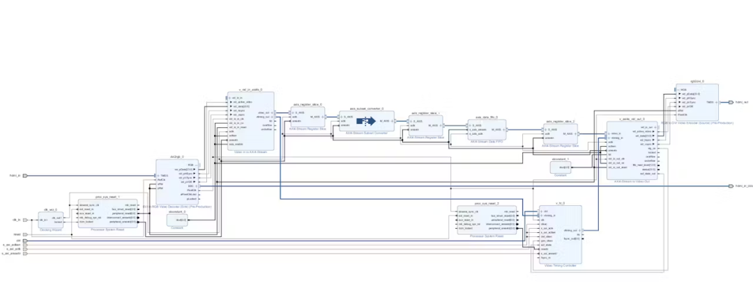
For this application, we will create an example image processing pipeline implemented using the direct method.
This means there is no frame buffering from input to output, ensuring minimal latency from input frame to output frame. To achieve this, we must minimize buffering throughout the pipeline.
Target Device
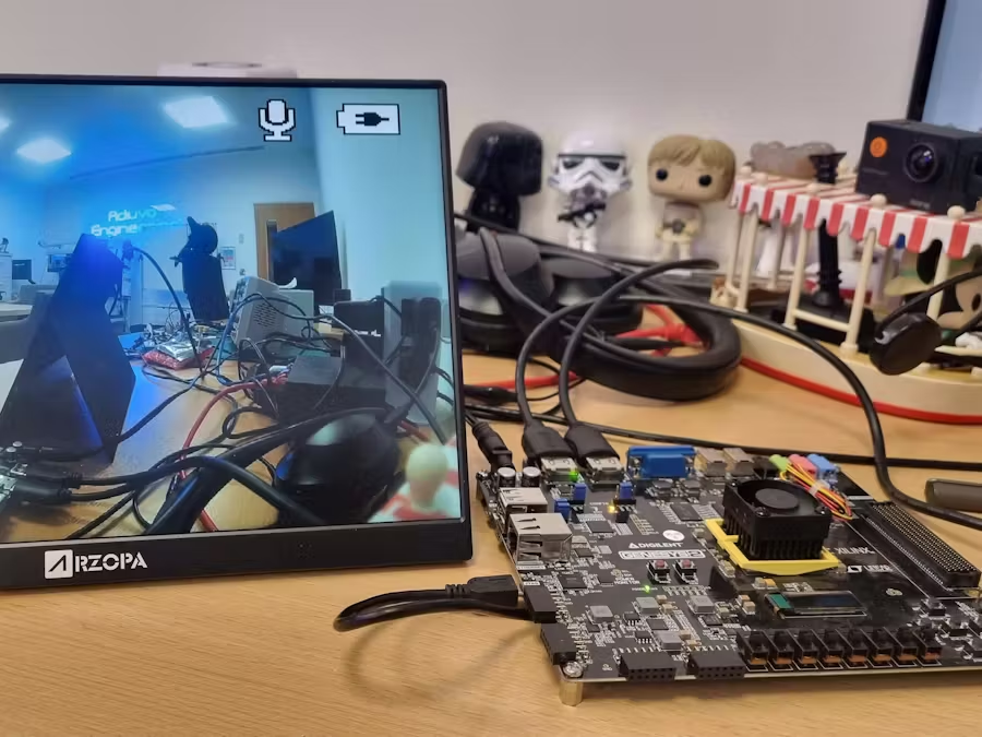
The target device for this design is the AMD Kintex™ 7 FPGA, specifically using the Digilent Genesys 2 development board, which features:
- HDMI input and output interfaces: Ideal for capturing images from action cameras or test devices and displaying them on a screen.
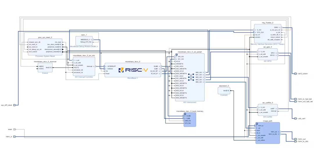
This design will utilize Vivado and can be divided into two main parts:
- Image Processing Pipeline
- Control and Configuration using AMD MicroBlaze V
Pipeline Design
The pipeline will:
- Receive data via HDMI: Convert it from a parallel video format with vertical and horizontal sync signals to AXI Stream.
- Convert the video stream to AXI Stream: AXI Stream is the standard interface used by most image processing blocks.
- Output data via AXI Stream to video output: This generates parallel video under the control of the video timing generator.
Control Using AMD MicroBlaze V Processor
The pipeline and associated video timing generator will be controlled by the AMD MicroBlaze V processor based on the RISC-V instruction set architecture.
Unlike previous examples using VDMA (Video Direct Memory Access), this application will not use VDMA to ensure the lowest latency between input and output.
AMD Vivado Design Suite Components
The image processing pipeline will use the following IP cores:
- DVI2RGB: Digilent IP core for converting DVI to RGB format.
- Video Input to AXI Stream: Vivado Design Suite IP block for converting RGB video to AXI Stream format.
- AXI Stream to Video Output: Vivado Design Suite IP block for converting AXI Stream back to RGB format.
- Video Timing Controller: Configured to detect input timing and generate output timing. If needed, this configuration will also support future VDMA applications.
- AXI Stream FIFO: Configured in packet mode, buffered before passing through the line.
- AXIS Register Slice: Added within the pipeline to assist with timing convergence.
AMD MicroBlaze V Processor Subsystem
The AMD MicroBlaze V processor controller subsystem is configured as a microcontroller. This configuration supports AXI peripheral data and instruction interfaces and connects via AXI interconnect to:
- UartLite: Vivado Design Suite IP block for UART console communication.
- AXI GPIO: Monitors hot-plug detection signals for the display and camera.
- AXI Interrupt Controller: Handles processor interrupts.
- MicroBlaze V Processor Debug Module: Supports debugging using the Vitis platform.
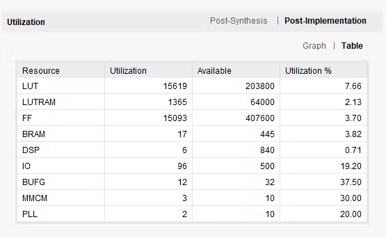
The device utilization is as follows:
The software runs on the AMD MicroBlaze V processor developed on the AMD Vitis platform.
#include <stdio.h>
#include "platform.h"
#include "xil_printf.h"
#include "xvtc.h"
#include "xgpio.h"
#include "vga.h"
#include "xparameters.h"

XVtc VtcInst;
XVtc_Config *vtc_config ;
XGpio hpd_in;
XVtc_SourceSelect SourceSelect;

int main()
{
    u16 result;
    VideoMode video;
    XVtc_Timing vtcTiming;

    init_platform();

    printf("Setting up VTC\n\r");

    vtc_config = XVtc_LookupConfig(XPAR_XVTC_0_BASEADDR);
    XVtc_CfgInitialize(&VtcInst, vtc_config, vtc_config->BaseAddress);

     //configure and assert the HPD
    XGpio_Initialize(&hpd_in, XPAR_XGPIO_0_BASEADDR);
    XGpio_DiscreteWrite(&hpd_in,1,0x1);
    sleep(20);
    XGpio_DiscreteWrite(&hpd_in,2,0x1); ///needs time here

    video = VMODE_1280x720;
 vtcTiming.HActiveVideo = video.width; /**< Horizontal Active Video Size */
 vtcTiming.HFrontPorch = video.hps - video.width; /**< Horizontal Front Porch Size */
 vtcTiming.HSyncWidth = video.hpe - video.hps;  /**< Horizontal Sync Width */
 vtcTiming.HBackPorch = video.hmax - video.hpe + 1;  /**< Horizontal Back Porch Size */
 vtcTiming.HSyncPolarity = video.hpol; /**< Horizontal Sync Polarity */
 vtcTiming.VActiveVideo = video.height; /**< Vertical Active Video Size */
 vtcTiming.V0FrontPorch = video.vps - video.height; /**< Vertical Front Porch Size */
 vtcTiming.V0SyncWidth = video.vpe - video.vps; /**< Vertical Sync Width */
 vtcTiming.V0BackPorch = video.vmax - video.vpe + 1;; /**< Horizontal Back Porch Size */
 vtcTiming.V1FrontPorch = video.vps - video.height; /**< Vertical Front Porch Size */
 vtcTiming.V1SyncWidth = video.vpe - video.vps; /**< Vertical Sync Width */
 vtcTiming.V1BackPorch = video.vmax - video.vpe + 1;; /**< Horizontal Back Porch Size */
 vtcTiming.VSyncPolarity = video.vpol; /**< Vertical Sync Polarity */
 vtcTiming.Interlaced = 0;

    memset((void *)&SourceSelect, 0, sizeof(SourceSelect));
 SourceSelect.VBlankPolSrc = 1;
 SourceSelect.VSyncPolSrc = 1;
 SourceSelect.HBlankPolSrc = 1;
 SourceSelect.HSyncPolSrc = 1;
 SourceSelect.ActiveVideoPolSrc = 1;
 SourceSelect.ActiveChromaPolSrc= 1;
 SourceSelect.VChromaSrc = 1;
 SourceSelect.VActiveSrc = 1;
 SourceSelect.VBackPorchSrc = 1;
 SourceSelect.VSyncSrc = 1;
 SourceSelect.VFrontPorchSrc = 1;
 SourceSelect.VTotalSrc = 1;
 SourceSelect.HActiveSrc = 1;
 SourceSelect.HBackPorchSrc = 1;
 SourceSelect.HSyncSrc = 1;
 SourceSelect.HFrontPorchSrc = 1;
 SourceSelect.HTotalSrc = 1;
 XVtc_RegUpdateEnable(&VtcInst);
 XVtc_SetGeneratorTiming(&VtcInst, &vtcTiming);
 XVtc_SetSource(&VtcInst, &SourceSelect);
 XVtc_EnableGenerator(&VtcInst);
 XVtc_Enable(&VtcInst);

 XVtc_EnableDetector(&VtcInst);
 XVtc_Enable(&VtcInst);
 xil_printf("Video Mode = %i ", result);
 xil_printf("\n\r");

    printf("VTC Set Up\n\r");
    cleanup_platform();
    return 0;
}
Conclusion
The above is just an appetizer, and finally, I recommend a Image Processing White Paper:
https://github.com/suisuisi/FPGATechnologyGroup/blob/main/Adiuvo_Image_Processing_with_Programmable_Logic_WhitePaper(%E5%9B%BE%E5%83%8F%E5%A4%84%E7%90%86%E7%99%BD%E7%9A%84%E7%9B%AE).pdf
Disclaimer:This article is reproduced from the OPENFPGA public account,for issues related to content, copyright, and others, please contact the staff via WeChat (13237418207), and we will connect with you to delete it as soon as possible!Submissions/Recruitment/Advertising/Course Cooperation/Resource Exchange, please add WeChat: 13237418207
Previous Recommendations
Who says configuration is difficult? This article will help you easily master Xilinx 7 series FPGA configuration techniques
100 Questions on Basic Concepts of Electronic Design Explained (Questions 1-10)
Three Methods of FPGA Version Management: Which One Will You Choose?
“180-Day FPGA Development Online Practical Training Course – Fanyi”

ScanAddCustomerServiceWeChattoJointhe Group“toBringYouintoFanyiEducationOfficialTechnicalWeChatGrouptoCommunicateTechnicalQuestionsandInsights~