Click the blue text above to follow us!👆

Author/Nanxi Image/Original
Gold plating on PCBs is a printed circuit board that forms a nickel-gold bimetal layer on the surface through a chemical deposition process. The thickness of gold plating on PCBs usually refers to the thickness of the gold layer, rather than the thickness of the PCB substrate. The thickness of the gold layer varies under different processes and application scenarios:
Typical Thickness Range
Standard PCB: 0.05~0.1μm (compliant with IPC-4552A standard)
High-frequency circuits: 0.025~0.05μm (to reduce signal loss)
Military/Aerospace: 0.075~0.125μm (to enhance corrosion resistance)
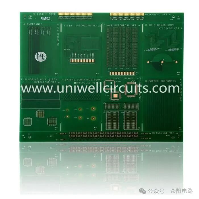 |
| (Zhonyang Circuit18L Gold Plated High TG PCBActual Image) |
The thickness range of gold plating on PCBs
The thickness of the gold plating process (chemical nickel-gold) generally consists of two parts:
Nickel layer thickness: As the base layer, the thickness is generally 120-240 microinches (μin), approximately 3-6 micrometers (μm), mainly providing mechanical strength and solder reliability.
Gold layer thickness: Covered on the nickel layer, the thickness range is narrow, usually 2-8 microinches (μin), approximately 0.05-0.2 micrometers (μm), used to protect the nickel layer from oxidation and ensure soldering performance.
Total thickness: The total thickness of gold plating on PCBs (nickel layer + gold layer) is generally between 3.05-6.2 micrometers (μm), depending on process requirements and cost considerations.
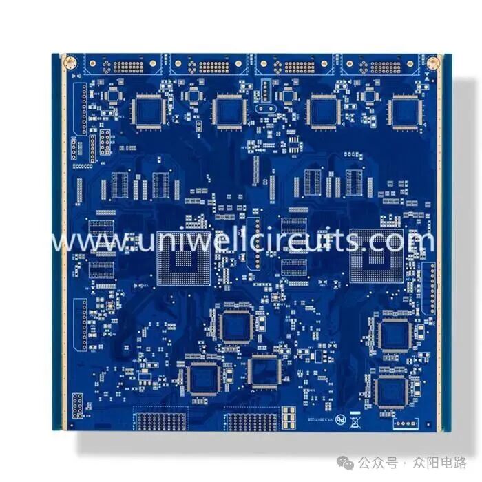 |
| (10-layer standard FR4 PCB) |
Cost and Performance Balance
For every additional 0.01μm of gold layer, the cost per board will also increase.Excessive thickness (>0.15μm) can lead to increased surface roughness, causing orange peel effect.
The thickness of the gold layer on PCB boards is usually 1-5 micrometers, achieved through electroplating, which can significantly enhance conductivity (reduce contact resistance), corrosion resistance (anti-oxidation), and soldering performance (enhance solder joint strength).Thickness directly affects reliability; for example: 3-5 micrometers is suitable for high-frequency signals or harsh environments (such as automotive electronics), while 1-2 micrometers is more commonly used for consumer low-cost products.Electroplating time can precisely control thickness, and it needs to balance cost and performance based on application scenarios (such as 5G communication, medical devices).
Generally Recommended Gold Plating Thickness
General scenarios: For most consumer electronics and industrial applications, a total thickness of 3-5 micrometers (μm) is sufficient to balance cost and performance.
High-reliability scenarios: For aerospace or high-frequency communication devices, a thicker gold layer (close to 8μin) may be required to enhance corrosion resistance and long-term stability.
Soldering optimization: A gold layer that is too thin (e.g., below 2μin) may lead to poor soldering or oxidation risks, while too thick (e.g., over 8μin) increases costs and may cause brittleness.
Typical Application Scenarios
High-end consumer electronics: Smartphone motherboards, wearable devices, rely on the flat surface of gold-plated boards for mounting small components.
High-frequency communication devices: 5G base stations, radar modules, utilize the low-resistance characteristics of the gold layer to reduce signal attenuation.
Industrial control: Automotive electronics, medical devices, require long-term stability to cope with vibration and temperature/humidity changes.
For more information about gold-plated PCBs, please contact us~
Why Choose Us
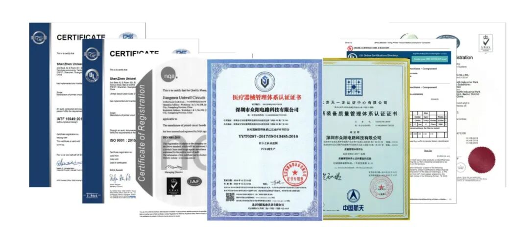
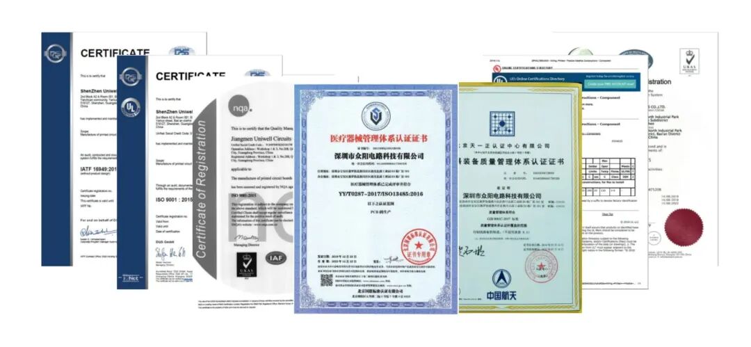
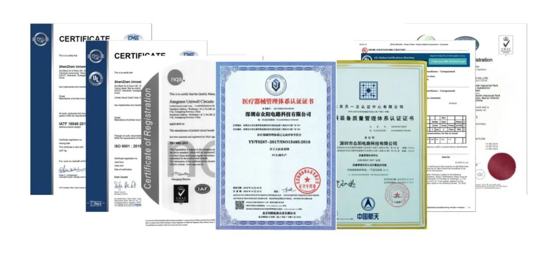
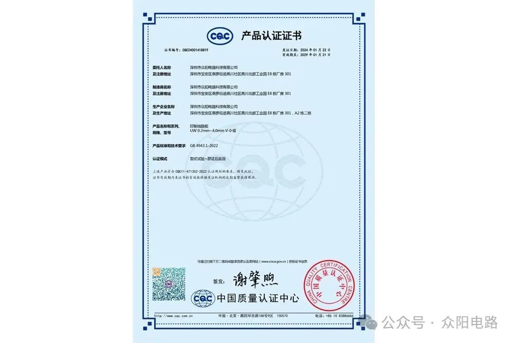
Manufacturer qualification certification is complete

–end–


Introduction to HDI Rigid-Flex Boards (Part 1)

Introduction to Back-drilling Technology

Ultra-thick Copper High Thickness Multi-layer Boards

Don’t forget to click

Share,

Collect,

View,

Like
Oh!