
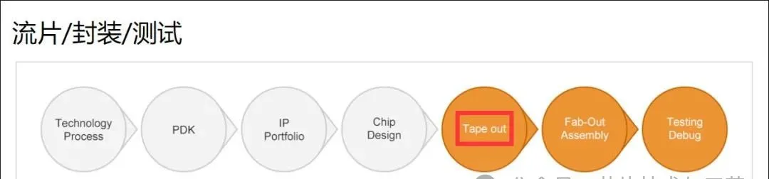
Chip tape out (Tape Out) technology is a core process in semiconductor manufacturing that accurately transfers design patterns to silicon wafers, serving as a critical bridge between design and production. This article comprehensively explores chip tape out technology, from design and tape out preparation to technical implementation, equipment, and material applications, analyzing key aspects and challenges in the tape out process.
|
|
|
|
|
|
|
|
|
|
|
|
|
|
|
|
|
|
|
|
|
|
|
|
Chip tape out is a critical process in semiconductor manufacturing, referring to the conversion of designed chip patterns from computer data into physical structures on actual silicon wafers. This process includes photolithography, etching, ion implantation, and metal deposition, ensuring the precise construction of integrated circuits on silicon wafers according to the design.

*Focused Ion Beam (FIB) technology is a technique that uses high-energy ion beams for micro-processing and analysis.
|
|
|
|
|
|
|
|
|
|
|
|
|
|
|
|
|
|
|
|
|
|
|
|
With the advancement of semiconductor technology, the chip tape out process continues to innovate. For instance, micro-milling technology has simplified the manufacturing process of microchannel chips, reducing production costs. The success of chip tape out relies on multi-faceted technical collaboration, such as the partnership between SMIC and CanSemi Semiconductor, which achieved the tape out of a 40nm low-leakage process ARM Cortex-A9 dual-core test chip, demonstrating the close cooperation between design, manufacturing, and testing stages.
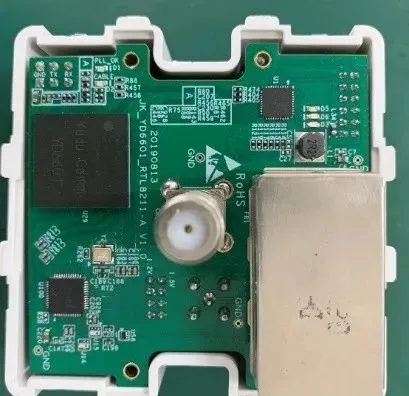
The importance of chip tape out technology in semiconductor manufacturing cannot be overlooked. It is not only the key process in transforming chip designs into actual products but also the driving force behind technological innovation and industrial development in the semiconductor industry. With advancements in technology and increasing market demand, chip tape out technology will continue to play its indispensable role.
Chip tape out occupies a significant position in semiconductor manufacturing; it is not only the key process that transforms chip designs into actual products but also serves as a bridge connecting design and production. Here are several aspects of its importance:
-
Realizing Chip Design Implementation: The tape out process transfers the designed chip pattern through a series of precise manufacturing steps onto silicon wafers, forming integrated circuits with specific functions. The success of tape out means that the designed chip can be smoothly transformed into a tangible product in the market, directly impacting the chip product’s launch and market competitiveness. -
Process Optimization and Cost Control: Process optimization and cost control during the tape out process are crucial for the market competitiveness of chips. With the development of semiconductor technology, the complexity and costs of chip manufacturing are also rising. By optimizing processes, production costs can be reduced, and production efficiency improved, making chip products more competitive in the market. Meanwhile, strict cost control ensures the profitability of chip products. -
Driving Technological Advancement: Continuous advancements in tape out technology provide strong support for the development of the semiconductor industry. With the advancement of Moore’s Law, the integration of integrated circuits has increased, placing higher demands on tape out technology. Adopting more advanced process technologies and introducing new materials and processes not only enhance the performance of chip products but also expand the application areas and market space of the semiconductor industry.
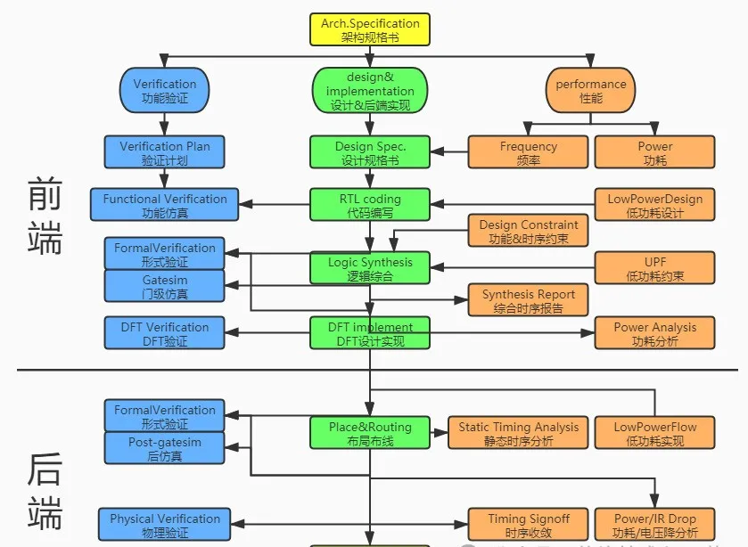
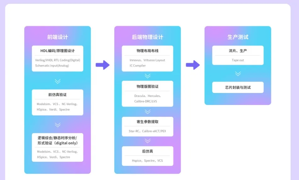
The chip design process is a complex and detailed procedure that encompasses multiple stages from functional definition to physical layout generation, typically divided into front-end design and back-end design.
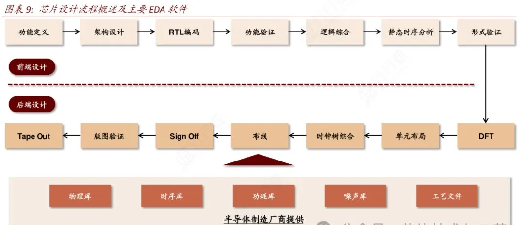
Front-End Design is the starting point of chip design, with the main goal of defining the chip’s functions and architecture. During this phase, the design team conducts detailed requirements analysis to clarify the specific functions the chip needs to achieve and writes RTL (Register Transfer Level) code. RTL code describes the internal logic structure of the chip, including data paths and control paths, as well as the interaction between various components. To ensure the correctness of the design, the front-end design phase also undergoes simulation verification to check whether the design meets the requirements by simulating the chip’s behavior in actual working environments.
Back-End Design unfolds after the front-end design is completed, with the primary task of converting logical descriptions into actual physical layouts. Back-end designers plan the layout, determining the positions of functional modules on the chip to optimize performance and reduce power consumption. The routing phase follows, ensuring signals can be accurately transmitted between various modules. Timing analysis and signal integrity analysis are also critical stages that ensure the chip maintains stable performance under various working conditions. After these steps, the back-end design ultimately generates a complete physical layout, laying the foundation for chip manufacturing.
After the chip design is completed, it enters the crucial preparation phase before tape out. The work done in this phase is critical as it directly relates to the success of the chip tape out.
-
Design Rule Check (DRC): This is the primary step aimed at verifying whether the design meets the requirements of the manufacturing process. For example, during the layout and routing process, it must be ensured that all design elements comply with the size and spacing rules set by the manufacturer to avoid potential manufacturing issues. -
Layout Verification (LVS): This step ensures consistency between the design layout and the schematic by comparing the two, preventing design errors or deviations. -
Parasitic Parameter Extraction: Due to the presence of parasitic parameters such as resistance and capacitance, the actual performance of the chip may deviate from the design expectations. Therefore, this phase requires precise extraction of these parasitic parameters and corresponding compensation in the design to ensure that the chip performance post-tape out meets expectations. -
Communication with Tape Out Vendor: Determining specific process parameters, such as doping concentration and oxide layer thickness, which are key factors affecting chip performance. Material selection is also crucial, as the physical and chemical properties of different materials directly influence chip performance and reliability. -
Testing Scheme Development: Deciding how to conduct comprehensive performance and reliability testing on the post-tape out chip to ensure that the chip meets design requirements.
|
|
|
|
|
|
|
|
|
|
|
|
|
|
|
|
|
|
|
|
|
|
|
|
|
|
|
|
|
|
|
|
|
|
|
|
|
|
|
|
|
|
|

Wuxi Qixin Semiconductor Technology Co., Ltd. is a high-tech enterprise specializing in the research, development, production, and sales of intelligent production equipment for the chip industry. Established in 2020, it is located in the Wuxi Huishan Economic and Technological Development Zone. The company has received multiple honors such as Wuxi Huishan District Pioneer Talent and Wuxi Taihu Talent, and is a council member of the Wuxi Semiconductor Association. The core members of the company’s R&D team have over 20 years of experience in semiconductor equipment, possessing rich R&D experience in packaging processes and related equipment industrialization, holding multiple national-level technology invention, utility model patents, and software copyrights. The company has long-term collaborations with well-known domestic institutions such as Tsinghua University and the Chinese Academy of Sciences for industry-university-research cooperation.
The self-developed MGP intelligent chip packaging system, AM fully automatic chip packaging system, TF unit modular chip automatic cutting and forming system, and other intelligent production equipment for chips have all been recognized by the market and received unanimous praise from customers.
Wuxi Qixin Semiconductor Technology Co., Ltd. adheres to the values of innovation, efficiency, quality, and integrity, based in Wuxi, with the mission of creating intelligent equipment for China’s independent chip brands, aiding the chip industry, and building smart factories. It aims to become a leader in the chip packaging and testing equipment industry!