Introduction
Let’s talk about the aspects of chip design, tapeout, validation, manufacturing, and costs; tapeout is like taking a major exam for chip design.
The importance of tapeout lies in its ability to verify whether the chip design is successful, making it a key step in chip manufacturing, where the finalized design is sent to the chip manufacturing plant to produce samples. It checks whether the designed chip meets the requirements or if further optimization is needed; if a compliant chip can be produced, then mass production can begin.

The input of the process shown in the image is the chip project design, and the output is the completed chip wafer.
1. Wafer Terminology
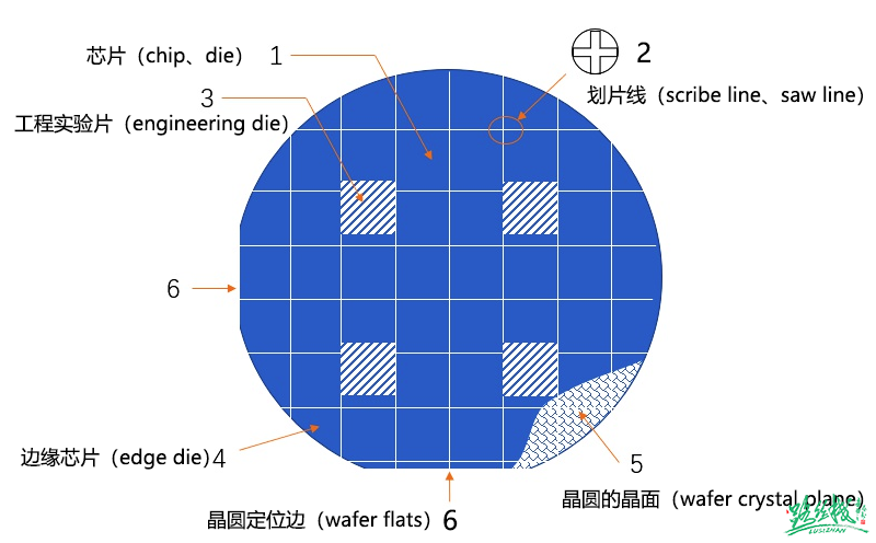
1. Chip (chip, die), device (device), circuit (circuit), microchip (microchip), or barcode (bar): All these terms refer to the microchip patterns that occupy most of the wafer’s surface area;
2. Scribe line (scribe line, saw line) or street (street, avenue): These areas are used to separate the gaps between different chips on the wafer. Scribe lines are usually blank, but some companies place alignment marks or testing structures in the gap areas;
3. Engineering die and test chip: These chips differ from production chips or circuit chips. They include special devices and circuit modules for electrical testing during the wafer manufacturing process;
4. Edge die: These are chips located at the edge of the wafer, where some mask defects occur, resulting in area loss. More edge waste caused by larger individual chip sizes can be compensated by using larger diameter wafers. One of the motivations driving the semiconductor industry to larger diameter wafers is to reduce the area occupied by edge chips;
5. Wafer crystal plane: The cross-section in the image indicates the lattice structure beneath the device. The orientation of the device edge relative to the lattice structure is determined;
6. Wafer flats/notches: The illustrated wafer has major flats and minor flats, indicating that this is a P-type <100> oriented wafer. Both 300mm and 450mm diameter wafers use notches as lattice orientation markers. These flats and notches also assist in wafer alignment in some wafer manufacturing processes.
2. Chip Tapeout Methods (Full Mask, MPW)
Full Mask and MPW are both methods of tapeout (sending design results for manufacturing) in integrated circuits. Full Mask means that all masks in the manufacturing process serve a specific design; MPW stands for Multi Project Wafer, which literally means multiple projects sharing a single wafer, allowing multiple IC designs to be manufactured in the same process.
1. Full Mask means that all masks in the manufacturing process serve a specific design; chips with Full Mask can produce thousands of dies from one wafer, which can then be packaged into chips to meet large-scale customer demand.
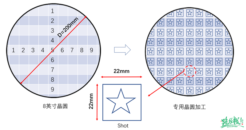
2. MPW, short for Multi Project Wafer, is similar to PCB panel prototyping, allowing multiple integrated circuit designs that use the same process to be placed on the same wafer for tapeout. After manufacturing, each design can obtain dozens of chip samples, which is sufficient for experiments and testing during the prototype design phase. This method can reduce tapeout costs by 90%-95%, significantly lowering chip R&D costs.
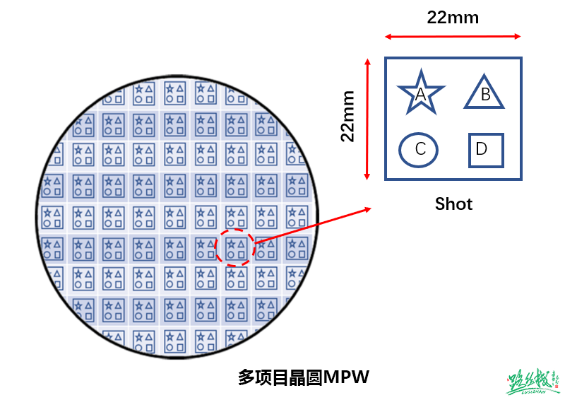
Wafer fabs have a fixed number of MPW opportunities each year, known as Shuttle, which operates on a schedule. Different companies share wafers based on certain rules, and MPW is limited by the number of SEATs allocated to each company, typically defined as a 3mm*4mm area. Wafer fabs generally limit the number of SEATs reserved for each company to ensure participation from various chip companies (having too many SEATs would increase costs and negate the purpose of MPW). The advantage of MPW is its lower tapeout cost, usually just a few hundred thousand, which significantly reduces risk; however, it should be noted that from a production perspective, MPW is a complete manufacturing process, thus it still takes time. A typical MPW takes about 6 to 9 months, which can delay chip delivery times.
Since it is a shared wafer, the number of chips obtained from MPW will be limited, primarily used for internal validation testing by chip companies, and may be provided to a very small number of top customers. From this, it can be understood that MPW is an incomplete, non-mass-producible tapeout.
3. Introduction to MPW from the perspective of wafer production
Chip processing is still a relatively complex process. I believe many friends, after reading the wafer structure understood by the first and second authors, visualize it as shown in the following image, where a frame belongs to a chip company.
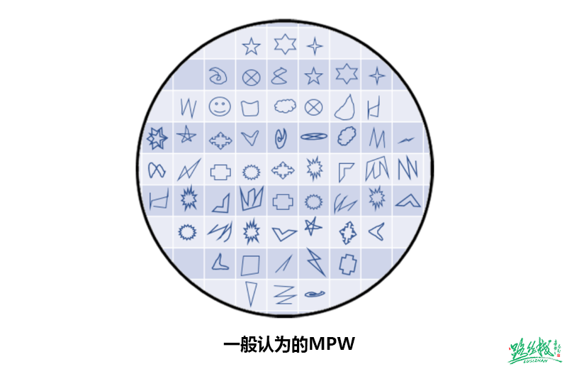
However, this is not the case, as it relates to the photolithography technology in the wafer production process; current photolithography technologies such as DUV/EUV mostly use reduction methods for exposure, as shown in the following image:
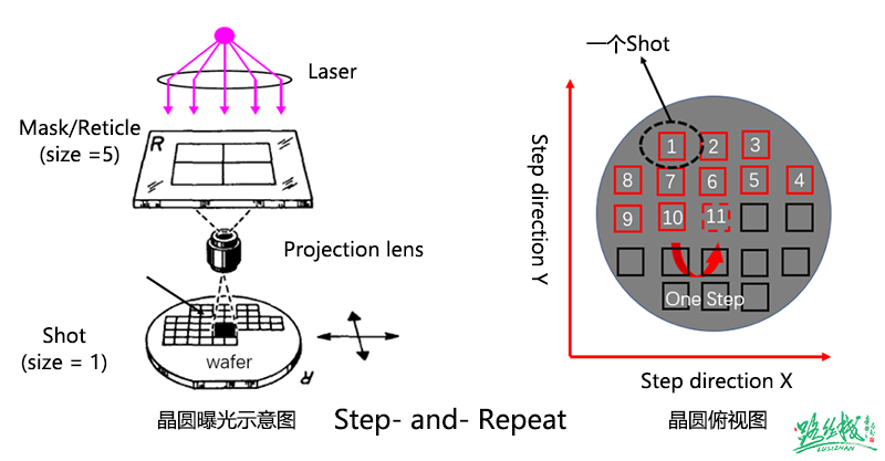
Using a 1:5 magnified mask for wafer exposure, the rectangular area exposed at one time is usually called a shot. After exposure, the photolithography machine automatically adjusts the wafer position for the next shot, repeating this process (Step-and-Repeat) until the entire wafer is exposed. The area of one shot is the region shared among users for SEAT allocation;
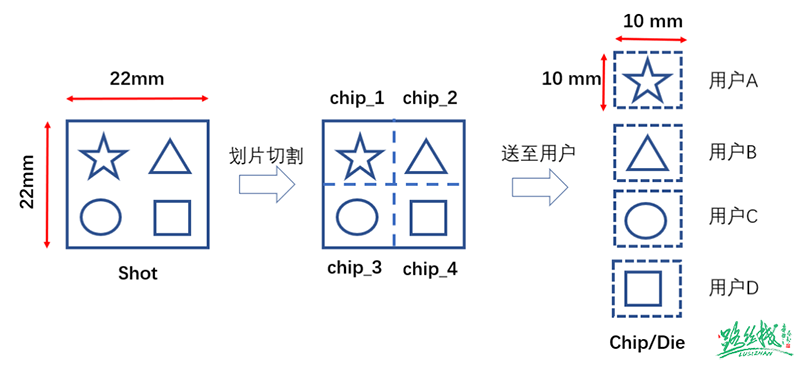
As illustrated, one shot is divided into four small grids, with each grid allocated to a vendor’s design. MPW wafers typically accommodate up to 20 users.
3. Chip ECO Process
ECO stands for Engineering Change Order, which refers to engineering change instructions. ECO can occur before, during, or after tapeout; ECO after tapeout may involve minor changes requiring only a few Metal layers or major changes requiring modifications to several Metal layers, or even a complete tapeout. The implementation process for ECO is illustrated in the following image:
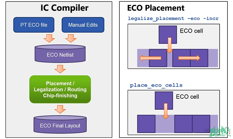
If chips from MPW or Full Mask show functional or performance defects during validation, ECO can be used for minor adjustments to the circuit and standard cell layout, allowing for small-scale optimizations while maintaining the original design layout and routing results, ultimately meeting the chip approval standards. Violations cannot be fixed through the backend layout routing process (repeating the entire process is too time-consuming) but must be addressed through the ECO process to optimize timing, DRC, DRV, and power consumption.
4. Tapeout Corners
1. Corners in chip manufacturing are physical processes that experience process variations (including doping concentration, diffusion depth, etching extent, etc.), leading to differences between batches, between different wafers of the same batch, and between different chips on the same wafer.
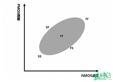
On a wafer, it is impossible for the carrier drift velocity to be the same at every point; as voltage and temperature vary, their characteristics will also differ. Classifying them leads to PVT (Process, Voltage, Temperature), with Process further divided into different corners: TT: Typical N Typical P FF: Fast N Fast P SS: Slow N Slow P FS: Fast N Slow P SF: Slow N Fast P The first letter represents NMOS, and the second letter represents PMOS, both referring to different concentrations of N-type and P-type doping. NMOS and PMOS are fabricated independently, without affecting each other, but in circuits, NMOS and PMOS operate simultaneously, which can result in scenarios where NMOS is fast while PMOS is also fast or slow, leading to the four conditions FF, SS, FS, and SF. Adjustments made through Process simulate the speed of devices, with different levels of FF and SS set based on the magnitude of deviations. Typically, most are TT, and the five corners mentioned above can cover about 99.73% of the range within +/-3 sigma, which follows a normal distribution.
2. The significance of corner wafers during engineering tapeouts is that fabs will adjust critical layers to account for inline variation, and some may use backup wafers to ensure that shipped wafers meet target specifications, especially near the TT corner. If samples are merely being produced, corner verification may not be necessary, but for subsequent mass production preparations, corners must be considered. Since process deviations occur during production, corner verification is required to estimate normal fluctuations in the production line, and fabs will have corner verification requirements for mass-produced chips. Therefore, designs must satisfy corner conditions, ensuring that circuits function normally under various corner and extreme temperature conditions to maximize the yield of the final produced chips.
3. Corner Split Table strategy For products, generally, corners must meet specifications. Typically, specifications have 6 sigma, where FF2 (or 2FF) indicates a shift towards the fast direction by 2 sigma, and SS3 (or 3SS) indicates a shift towards the slow direction by 3 sigma. Sigma primarily reflects the fluctuation of Vt; larger fluctuations lead to larger sigma. Here, 3 sigma is within the specification line of the process device, allowing for slight deviations since fluctuations cannot perfectly align with the specification.
The following is an example of a corner split table for a 55nm Logic process:
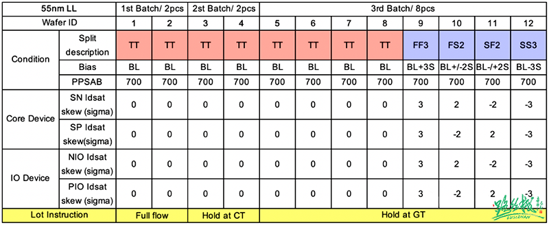
① #1 & #2 two pilot wafers, one blind sealed, one for CP testing;
② #3 & #4 two wafers held at Contact, reserved for later modifications, saving ECO tapeout time;
③ #5 to #12 eight wafers held at Poly, waiting for pilot results to determine if device speed needs adjustment and to verify corners;
④ In addition to reserving enough chips for testing and verification, Metal Fix, as much as possible, wafers should be reserved for mass production shipments based on project needs.
4. Confirming Corner Results
First, most should fall within the window range determined by the four corners; significant deviations may indicate process shifts. If the yield of each corner meets expectations, it indicates sufficient process window. If individual conditions yield low results, the process window needs adjustment. The purpose of corner wafers is to verify design margins and assess yield loss. Generally, chips exceeding the performance range of this corner constraint are scrapped.
Corner verification is benchmarked against WAT test results, generally led by fabs, but the costs of corner wafers are borne by design companies. For mature and stable processes, chips on the same wafer, from the same batch, or even different batches have very similar parameters, and the deviation range is relatively small. Process corners (Process Corner) PVT (Process Voltage Temperature) process errors differ significantly between different chips and batches, unlike bipolar transistors.
To alleviate the difficulties of circuit design tasks, process engineers must ensure that device performance remains within a certain range. Generally, they strictly control expected parameter variations by scrapping chips that exceed this performance range.
① The speed of MOS transistors corresponds to the threshold voltage. Fast corresponds to a low threshold voltage, while slow corresponds to a high threshold voltage. GBW=GM/CC, under identical conditions, a lower vth results in a higher gm value, thus increasing GBW and speed (specific situations require specific analysis).
② The speed of resistors. Fast corresponds to a lower square resistance, while slow corresponds to a higher square resistance.
③ The speed of capacitors. Fast corresponds to the smallest capacitance, while slow corresponds to the largest capacitance.
5. Tapeout Costs and Wafer Prices
The mask cost for 40nm tapeout is approximately $800,000 to $900,000, with wafer costs around $3,000 to $4,000 each. Including IP merge, it can easily exceed 7-8 million RMB.
28nm process tapeout costs $2 million per instance; 14nm process tapeout costs $5 million; 7nm process tapeout costs $15 million; 5nm process tapeout costs $47.25 million; and 3nm process tapeout may exceed $100 million; among the major tapeout costs, masks are the most expensive.
The more advanced the process node, the more mask layers are required; each mask corresponds to a coating of photoresist, exposure, development, etching, etc., involving material costs and equipment depreciation costs, all of which must be borne by fabless customers!
40 layers are needed for 28nm, 60 masks for 14nm; 80 or even over a hundred masks for 7nm; each mask costs $80,000, so chips must be mass-produced to lower costs!
Taking 40nm MCU process as an example: If 10 wafers are produced, the cost per wafer is (900,000 + 4,000*10)/10 = $94,000; if 10,000 wafers are produced, the cost per wafer is (900,000 + 4,000*10,000)/10,000 = $4,090. (The larger the wafer volume, the cheaper it is; different manufacturers also have different quotes.)
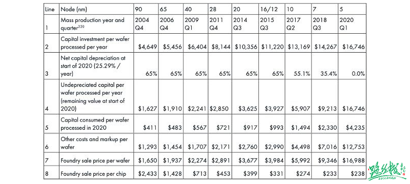
Wafer foundry prices are sourced from the internet
Taiwan Semiconductor Manufacturing Company (TSMC) provided the latest quote this year: for the most advanced 3nm process, each wafer costs $19,865, approximately 142,000 RMB.
Conclusion
There are several important stages from chip design to finished product: design -> tapeout -> packaging -> testing, but the cost composition of chips varies significantly, typically comprising 20% labor cost, 40% tapeout, 35% packaging, and 5% testing.
Tapeout is a high-risk endeavor, with risk probabilities ranging from 15% to 35%; these probabilities vary between teams and chip types. Some analog chip companies, even with complete teams and clear ideas, took 8 years and went through 18 tapeouts to finally complete the validation of sensor analog computation IP, creating the ideal ultra-low power, ultra-close transmission chip.
Chip R&D requires not restlessness and noise, but patience! (WeChat:一路上 18620364816)