
Click the blue text to follow us

In hardware and embedded development, the terms chip, module, and development board are often mentioned. What are they, and what is their relationship? In this article, we will use Espressif’s ESP32 as an example to explain the relationship among these three.
Overall, from chips to modules to development boards, they represent a progressive hierarchy, requiring increasingly more hardware resources.
In terms of appearance, the chip itself is very small; even when packaged, it is usually only the size of a fingernail. For example, the ESP32-S3 chip is packaged using QFN56 (QFN is a quad flat no-lead package technology, and 56 refers to the number of pins), with a size of only 7mm✕7mm.
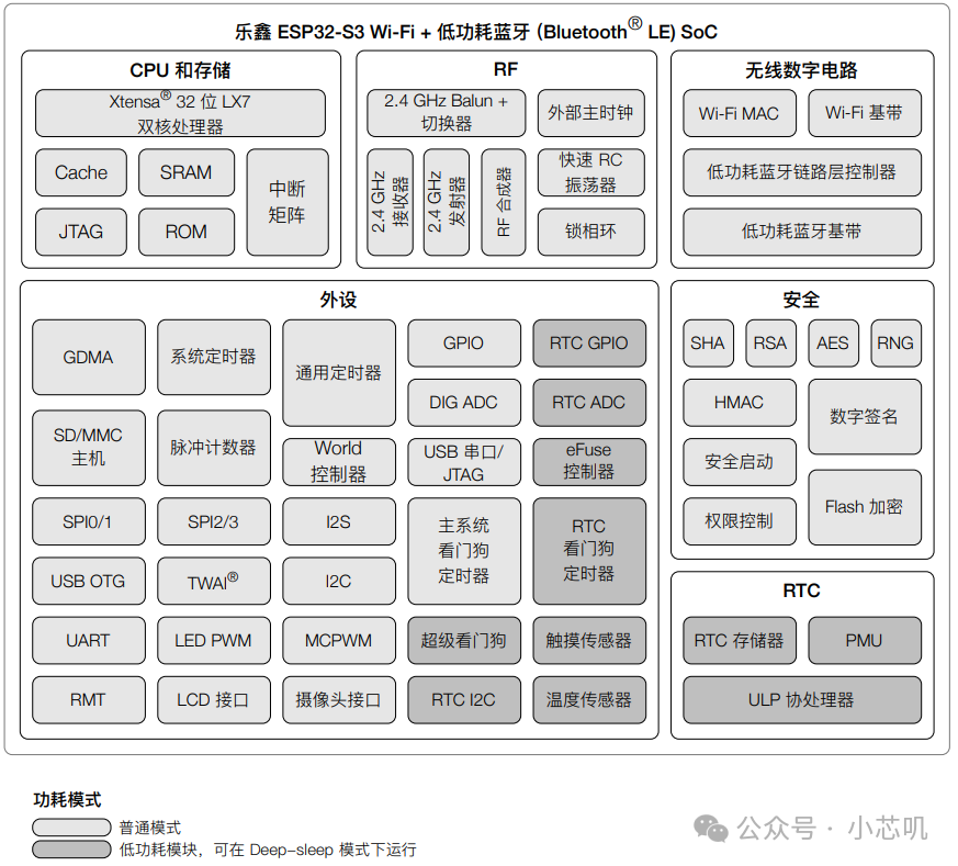
Functional block diagram of the ESP32-S3 chip
The chip integrates hardware circuits that implement specific functions. For instance, the ESP32-S3 is a low-power MCU, which integrates a dual-core Xtensa 32-bit LX7 processor, ultra-low power co-processor, Wi-Fi baseband, Bluetooth baseband, RF module, and a rich set of peripherals.
The chip is the foundation for implementing all hardware functions, but it is not a finished product intended for end-user use; it must be paired with peripheral components such as clock sources, resistors, capacitors, and antennas to function, which together form a module.
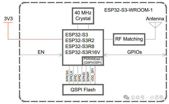
Functional block diagram of the ESP32-S3-WROOM-1 module
As can be seen, the ESP32-S3-WROOM-1 module not only includes the ESP32-S3 chip but also adds a 40MHz crystal oscillator, RF matching circuit, antenna, QSPI Flash, GPIO expansion, power supply, and enable circuit.
-
40MHz Crystal Oscillator:
Provides a stable clock signal for the ESP32-S3 chip.
-
RF Matching Circuit:
Achieves impedance matching for RF signals, allowing Wi-Fi and Bluetooth RF signals to be efficiently transmitted between the chip and the antenna.
-
Antenna:
Responsible for transmitting and receiving Wi-Fi and Bluetooth signals.
-
QSPI Flash:
Used for storing program firmware, user data, etc.
-
GPIO Expansion:
Standardizes the GPIO pins of the ESP32-S3 chip for easy connection to external devices.
-
Power Supply:
Provides a stable 3.3V operating voltage for the module.
-
Enable Circuit:
Used to control the power-up and reset of the chip.
Although the module can make the chip usable, it is difficult for developers to use due to the lack of standardized debugging interfaces and visual feedback functions, which is why the design core of the development board is to optimize a series of issues for the module, enabling developers to achieve efficient development.
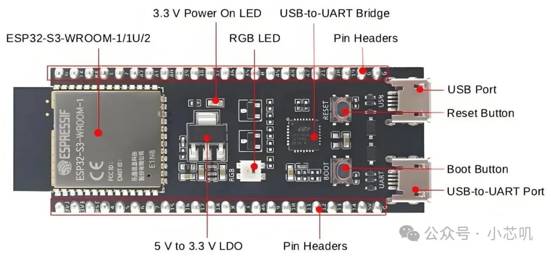
The ESP32-S3-DevKitC-1 development board is developed based on the ESP32-S3-WROOM-1 module mentioned above, with the largest component on the left being the module. In addition to the module, the development board also adds a 5V to 3.3V LDO, pin headers, USB to UART interface, Boot button, Reset button, USB interface, USB to UART bridge, RGB LED, and a 3.3V power indicator.
-
5V to 3.3V LDO:
Converts external 5V power supply to 3.3V to power the module and other circuits.
-
Pin Headers:
The development board exposes all GPIO pins through pin headers, allowing developers to connect them to sensors, displays, and other peripherals.
-
USB to UART Interface:
The Micro-USB interface can be used as a power supply interface for the development board, to flash firmware to the chip, and as a communication interface to communicate with the chip via the USB to UART bridge.
-
Boot Button:
Download button.
-
Reset Button:
Reset button.
-
USB Interface:
The USB interface can be used as a power supply interface for the development board, to flash firmware to the chip, to communicate with the chip via USB protocol, and for JTAG debugging.
-
USB to UART Bridge:
Enables serial communication between the computer and the module, providing a transmission rate of 3Mbps.
-
RGB LED:
A tri-color LED that provides visual function debugging and status indication.
-
3.3V Power Indicator:
The indicator lights up when the development board is connected to a USB power source.
Therefore, the chip is the cornerstone for implementing all hardware functions, the module transforms the chip’s capabilities into usable functions by adding peripheral circuits, and the development board is specifically designed for hardware developers, adding visual feedback, standardized interfaces, and debugging tools on top of the module, significantly lowering the barrier to hardware development.
Thank you for reading my article. If you find it useful, please give me a follow. Let’s chat again next time.
>/ Author: Xiao Xin Ji