Article Information
Title (Chinese): Flexible Embedded Metal Meshes Based on Nanosphere Lithography for Very Low Sheet Resistance Transparent Electrodes and EMI ShieldingPaper Title (English): Flexible Embedded Metal Meshes by Nanosphere Lithography for Very Low Sheet Resistance Transparent Electrodes, Joule Heating, and Electromagnetic Interference ShieldingAuthors: Mehdi Zarei, Khashayar Mohammadi, Abdullah A Mahmood, Mingxuan Li, Paul W. Leu*Affiliations: Department of Mechanical Engineering/Industrial Engineering, University of Pittsburgh; Department of Civil Engineering, University of WaterlooJournal: ACS Applied Electronic Materials, 2025, Vol.7, 4266−4278DOI: 10.1021/acsaelm.5c00425
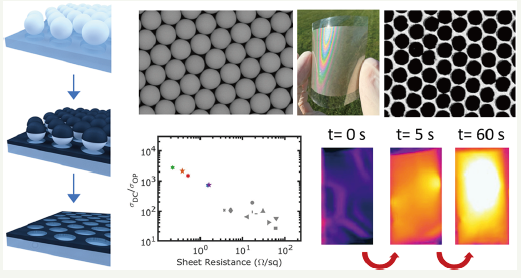
Summary
This study successfully demonstrates the first implementation of embedded nanosphere lithography metal meshes, achieving the highest performance for transparent electrodes to date and the first application of transparent EMI shielding, with a sheet resistance as low as 0.22 Ω/sq, improving the Figure of Merit (FoM) by an order of magnitude.
Research Background and Scientific Issues
- Transparent conductive electrodes (TCE) are widely used in OLEDs, displays, solar cells, etc., but traditional ITO suffers from high brittleness, high cost, and insufficient flexibility.
- Alternative materials such as silver nanowires and graphene show promise but face issues of unstable conductivity and high contact resistance.
- Metal meshes have garnered attention for their high transparency and conductivity, but conventional fabrication methods like photolithography and 3D printing are costly and have limited resolution.
- Nanosphere lithography (NSL) is a simple and low-cost process, but previously fabricated mesh electrodes had limited performance, with FoM rarely exceeding 100.
Core Challenge: How to maintain high transparency while achieving extremely low sheet resistance and excellent mechanical stability?
Technical Principles and Innovations
- Using nanosphere lithography + reactive ion etching (ICP-RIE) to etch “grooves” on PET/glass substrates, followed by silver deposition and removal of the sphere layer, forming high aspect ratio embedded metal meshes.
- Innovations:
- Embedded Design → The mesh is embedded in the substrate rather than on the surface, improving adhesion and mechanical durability.
- Thickness Breakthrough → NSL is typically limited to 50 nm films, while this study achieves thicknesses of 150–900 nm.
- Performance Exceeding an Order of Magnitude → FoM reaches up to 2736 (conventional NSL does not exceed 100), marking the first application of transparent EMI shielding.
Experimental Validation and Performance
- Transparent Electrode Performance:
- PET substrate: sheet resistance 1.52 Ω/sq (T=73.1%), FoM=737;
- After further optimization, sheet resistance 0.22 Ω/sq (T=58.1%), FoM reaches 2736.
- Transparent EMI Shielding:
- SE=34.5 dB (T=73.1%);
- SE=52.8 dB (T=58.1%), marking the first EMI shielding achieved through NSL meshes.
- Mechanical Durability:
- After 1000 bends, sheet resistance only increased by 0.1–0.3 Ω/sq;
- 60 tape peel tests showed almost no degradation.
- Heating Performance (Joule Heating):
- At 1.2 V, temperature rises to 70 °C within 60 seconds, demonstrating rapid thermal response capability.
Academic Contributions
- Theory: Proposed a new configuration for embedded high aspect ratio meshes, breaking through the limitations of NSL.
- Method: First application of nanosphere lithography for the fabrication of high-performance transparent EMI shielding structures.
- Experiment: Achieved record-level performance in both sheet resistance and FoM, and validated multifunctionality such as bending and heating.
- Application: Provides a new TCE pathway for OLEDs, solar cells, electric heaters, and transparent shielding materials.
Limitations and Future Directions
- Current experiments primarily use 3 μm microspheres, which have some arrangement defects and cracks, affecting optical uniformity;
- Future work could optimize sphere assembly processes or explore smaller diameters/multilayer structures for high-resolution optoelectronic devices;
- Future applications may expand to automotive window heating and defogging, flexible displays, and smart wearables.
Conclusion
This work demonstrates a low-cost, scalable, and breakthrough performance embedded metal mesh transparent conductive electrode, marking the first entry of NSL technology into the fields of EMI shielding and flexible heating applications. For researchers in optoelectronics and energy devices, this study provides a new material solution that combines high conductivity, flexibility, and functional integration.
Image Appreciation (Partial Examples)
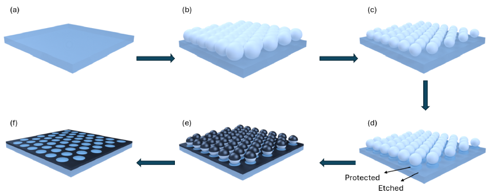
Figure 1. Schematic of the preparation process for embedded Ag mesh: Including substrate cleaning, PS microsphere deposition, O₂ plasma etching, ICP-RIE groove processing, electron beam deposition of Ag, and microsphere removal.
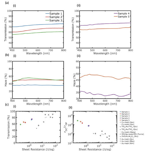
Figure 3. Optical and electrical performance:(a) Visible light transmittance curve;(b) Haze variation curve;(c) Outstanding performance of the samples in transmittance-sheet resistance and FoM-sheet resistance coordinates.
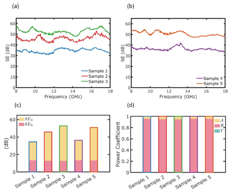
Figure 5. EMI shielding performance:(a, b) Shielding effectiveness of PET and glass samples in the 8–18 GHz frequency range;(c) Reflection/absorption contribution breakdown;(d) Power coefficient comparison.
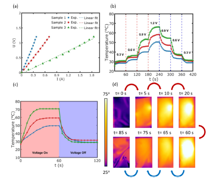
Figure 7. Joule heating performance:(a) I–V curve indicating ohmic behavior;(c) Rapid temperature rise to 70 °C at 1.2 V;(d) Infrared imaging revealing heating uniformity.

🔗 Contact Us
Official Website tssphere.com
Scan the QR code to contact customer service:

Taobao Store QR Code