

What is a semiconductor? Is it a material with electrical conductivity between that of a conductor and an insulator at room temperature? Does this explanation make sense to everyone? Can it generate interest among people from different industries? This article will provide a multi-dimensional explanation of the semiconductor industry, making it more than just a material viewed by physicists and chemists, which has conductivity between conductors and insulators at room temperature. It is also not merely the core hardware of the electronic information industry for entrepreneurs and manufacturers, including four major categories: integrated circuits, optoelectronic devices, discrete devices, and sensors. Additionally, it is not just an academic discussion of the semiconductor industry chain, which includes the upstream semiconductor industry represented by integrated circuits, the midstream electronic components and modules industry, and the downstream assembly and terminal application industry. The article aims to analyze semiconductors from as many angles as possible based on the author’s understanding of the materials, allowing more readers to find points of interest in semiconductors from their familiar perspectives.
1. Understanding Semiconductors from the Perspective of Physical and Chemical Materials
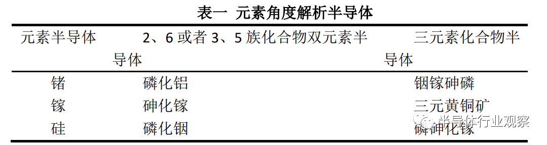
A semiconductor refers to a material with electrical conductivity between that of a conductor and an insulator at room temperature. Semiconductors are generally divided into two categories: elemental semiconductors and compound semiconductors, which are derived from group 4 elements and groups 2 and 6 of the periodic table, respectively. Semiconductors can also be classified based on the number of constituent elements, such as binary compound semiconductors and ternary compound semiconductors.
1.1. Elemental Semiconductors
Elemental semiconductors are composed of a single element, including boron, germanium, silicon, gray tin, antimony, selenium, tellurium, etc. Among these, germanium, silicon, and tin have been researched earlier, and their preparation processes are relatively mature. The position of elemental semiconductor materials in the periodic table explains the relationship between the properties of semiconductor materials and the structure of substances, especially atomic structure, as they all belong to group A in the periodic table. Elements with semiconductor properties include silicon, germanium, boron, selenium, tellurium, carbon, iodine, etc.
Their conductivity lies between that of conductors and insulators, typically with resistivity ranging from 10-7 to 10-3. They are mainly prepared using methods such as the Czochralski method, zone melting method, or epitaxy. The most widely used in industry are silicon, germanium, and selenium, which are utilized in various applications such as transistors, rectifiers, integrated circuits, and solar cells. Other materials like boron, carbon (diamond, graphite), tellurium, iodine, red phosphorus, gray arsenic, gray antimony, gray lead, and sulfur are also semiconductors but have not yet been applied.
1.2. Binary Compound Semiconductors from Groups II-VI or III-V
Binary compound semiconductors from groups II-VI or III-V refer to compounds formed by two defined atomic ratios, possessing specific bandgap widths and energy band structures. This includes crystalline inorganic compounds (like III-V and II-VI compound semiconductors) and their solid solutions, amorphous inorganic compounds (like glass semiconductors), organic compounds (like organic semiconductors), and oxide semiconductors. When we refer to compound semiconductors, we usually mean crystalline inorganic compound semiconductors.
The main binary compound semiconductors include:Gallium arsenide, indium phosphide, cadmium sulfide, bismuth telluride, and cuprous oxide. They are typically produced using methods such as the Bridgman method (a method for growing single crystals from the melt), liquid encapsulated Czochralski method, and vertical gradient freezing method. Their thin films and ultra-thin layer microstructured compound materials are prepared using epitaxy and chemical vapor deposition methods. They are used in optoelectronic devices, high-speed microelectronic devices, and microwave devices.
1.3. Ternary Compound Semiconductors
Ternary compound semiconductor materials are compounds formed by three defined atomic ratios, possessing specific bandgap widths and energy band structures. Broadly speaking, ternary compound semiconductors with ideal Eg values can be divided into two categories. The first category is what is commonly referred to as “pseudo-binary” compound semiconductors, which are formed by mixing two binary compounds, such as the ternary compound semiconductor GaxIn1-xAs (where 0≤x≤1, x represents the molar fraction of GaAs) made by mixing GaAs and InAs alloys. The semiconductor structures grown this way are disordered, and the alloy elements do not form regular crystals. The second category comprises true ternary compound crystals. For example, AIP can be considered as Si atoms in Si crystals being replaced by Al and P atoms; similarly, the ternary compound CuGaS2 can be viewed as the binary system ZnS being replaced, i.e., ZnS + ZnS → CuGaS2.
In a broad sense, ternary compound semiconductors with ideal Eg values can be divided into two categories. The first category is what is commonly referred to as “pseudo-binary” compound semiconductors, which are formed by mixing two binary compounds, such as the ternary compound semiconductor GaxIn1-xAs (where 0≤x≤1, x represents the molar fraction of GaAs) made by mixing GaAs and InAs alloys. The semiconductor structures grown this way are disordered, and the alloy elements do not form regular crystals. The second category comprises true ternary compound crystals. For example, AIP can be considered as Si atoms in Si crystals being replaced by Al and P atoms; similarly, the ternary compound CuGaS2 can be viewed as the binary system ZnS being replaced, i.e., ZnS + ZnS → CuGaS2.
1.4. In Summary
Elemental semiconductors are the earliest discovered and applied semiconductors, opening the door for humanity to use semiconductors, while binary and ternary compound semiconductors represent the development of the semiconductor industry. The differences between binary and ternary semiconductors are worth noting in several aspects:
(1) Volume change. The volume of the unit cell in a ternary compound structure does not equal the sum of the unit cell volumes of the two binary compounds. Generally, the volume change involves both a change in the cubic lattice constant a and a change in the ratio c/a.
(2) Chemical electronegativity. Due to the interaction and exchange of binding energy between A-C and B-C in the composite structure, the electronegativity of ternary compound semiconductors differs significantly from that of any of its binary compound components.
(3) Structural change. The composite structure of the two materials manifests as the mutual influence of binding forces, meaning they may combine in an optimal way without following the original binding rules.
(4) p-d orbital hybridization. Taking chalcopyrite as an example, in the composite structure system, there is a clear phenomenon where Zn (or Ga) obtains binding forces and energy gaps from the active 3d orbitals of Cu.
2. Understanding Semiconductors from the Product Perspective
Semiconductors are applied in integrated circuits, consumer electronics, communication systems, photovoltaic power generation, lighting, and high-power power conversion, with diodes being devices made from semiconductors. From both technological and economic development perspectives, the importance of semiconductors is immense. Most electronic products, such as computers, mobile phones, or digital recorders, have core components closely associated with semiconductors. Common semiconductor materials include silicon, germanium, and gallium arsenide, with silicon being the most influential among various semiconductor material applications. From a product perspective, semiconductors are the core hardware foundation of the electronic information industry, including four major categories: integrated circuits, optoelectronic devices, discrete devices, and sensors.
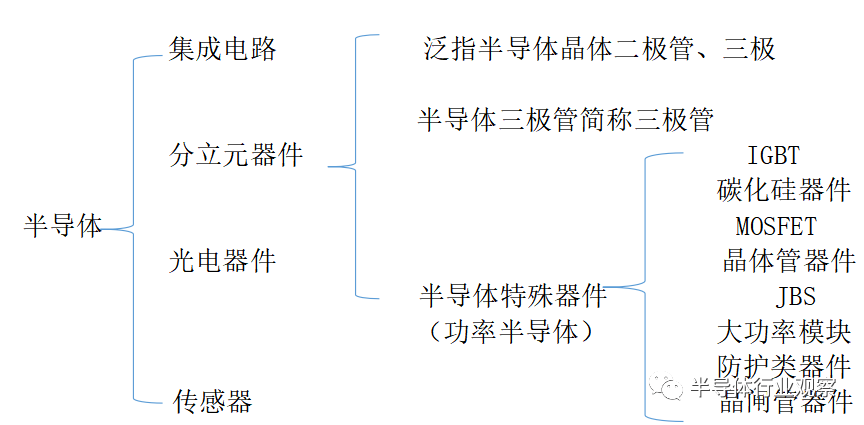
Figure 1: Product Perspective Analysis of the Semiconductor Industry
The largest market share is occupied by integrated circuits (over 80%), which can be further subdivided into analog chips, processor chips, logic chips, and memory chips. Therefore, when people discuss “integrated circuits,” they largely represent the concept of “semiconductors.”
In 2021, the global semiconductor industry sales reached $468.778 billion, a year-on-year increase of 8.72%; China’s semiconductor industry sales reached $258.1 billion, a year-on-year increase of 15.22%. From 2008 to 2018, China’s semiconductor industry rapidly expanded under the drive of national industrial policies and the development of downstream terminal application markets, increasing its share of the global semiconductor industry from 18.16% to 33.73%, highlighting its growing importance in the global semiconductor industry.
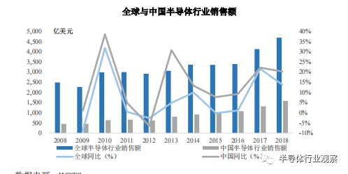
Figure 2: Global and China Semiconductor Industry Sales
Note: Image source from Hu Silicon Industry prospectus
2.1. Integrated Circuits
Integrated circuits (ICs) are miniaturized electronic devices or components. They are manufactured by interconnecting the required transistors, resistors, capacitors, and inductors of a circuit on a small piece or several small pieces of semiconductor wafers or substrate material using specific processes, and then packaged in a shell to form a microstructure with the required circuit function. All components are structurally integrated, making significant strides towards miniaturization, low power consumption, intelligence, and high reliability of electronic components.
According to the WSTS classification standard, semiconductor chips can be mainly divided into four categories: integrated circuits, discrete devices, sensors, and optoelectronic devices. Among them, integrated circuits can be further divided into memory, analog chips, logic chips, and microprocessors. Analog chips can be further subdivided into power devices, amplifiers, filters, feedback circuits, reference source circuits, and switched capacitor circuits. RF front-end chips are a type of analog chip that integrates various types of analog chips into a module. Today, most applications in the semiconductor industry are based on silicon integrated circuits. Integrated circuits play a crucial role in various industries and are the cornerstone of modern information society. The meaning of integrated circuits has far exceeded the definition at their inception, but their core aspect remains unchanged: “integration,” with various derived disciplines mainly revolving around the questions of “what to integrate,” “how to integrate,” and “how to handle the pros and cons of integration.” Silicon integrated circuits are mainstream, integrating all components required to achieve a specific function on a silicon chip, forming a whole called an integrated circuit.
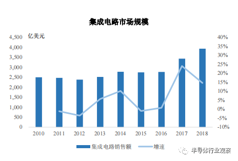
Figure 3: China’s Integrated Circuit Scale and Growth Rate
Note: Image source from Hu Silicon Industry prospectus
2.2. Optoelectronic Devices
Optoelectronic devices are devices made based on the photoelectric effect, also known as photo-sensitive devices. There are many types of optoelectronic devices, but their working principles are based on the physical foundation of the photoelectric effect. The main types of optoelectronic devices include phototubes, photomultiplier tubes, photoresistors, photodiodes, phototransistors, photovoltaic cells, and optocouplers. The conductivity of semiconductor materials is determined by the concentration of carriers. The carriers in semiconductor materials include free electrons within the material and the vacancies they leave behind—holes. Under normal conditions, the formation and recombination of free electrons and holes are in dynamic equilibrium. Electrons must overcome atomic binding to become free electrons, which requires energy, and light can provide energy to enhance their ability to break free from atomic binding. This disrupts the original dynamic equilibrium, causing the formation rate of free electrons and holes to exceed the recombination rate, thereby forming free electron-hole pairs within the semiconductor. Thus, light can change the carrier concentration, altering the conductivity of the semiconductor. The components of optoelectronic devices include six parts: first, photoresistors, which are the most commonly used in photodetectors; photoresistors have high resistance in the absence of light, and their resistance decreases significantly under illumination, enhancing conductivity. The main parameters of photoresistors are dark resistance, dark current, and their corresponding bright resistance and bright current. The greater the difference between bright and dark resistance, the better. When selecting photoresistors, attention must also be paid to their light and spectral characteristics; second, photodiodes, which operate in cutoff mode under no light conditions, similar to general diode characteristics, exhibiting unidirectional conduction. When illuminated, the carrier concentration in the PN junction increases significantly, forming photocurrent; third, phototransistors, which differ from ordinary transistors in that their emitter size is relatively small. When illuminated, the photocurrent is nearly equal to the base current of the ordinary transistor, and phototransistors are more sensitive than photodiodes; fourth, photovoltaic cells, with silicon photovoltaic cells being the most commonly used. They can directly convert light energy into electrical energy. A significant feature of photovoltaic cells is that the short-circuit current is linearly proportional to light intensity. In applications, a very small load resistance is generally selected. The smaller the load resistance, the better the linearity; fifth, phototubes, which are generally divided into vacuum phototubes and gas phototubes. Gas phototubes are typically filled with argon or argon-neon mixed gas, both of which are inert gases with relatively low atomic weights. The downside of gas phototubes is their rapid sensitivity decay; sixth, photomultiplier tubes, which consist mainly of a cathode chamber and a secondary emission multiplication system. The photoelectric characteristics of photomultiplier tubes show a linear relationship when light flux is low. The existence of dark current in photomultiplier tubes limits their minimum measurement range.
2.3. Discrete Devices
Discrete devices are widely used in consumer electronics, computers and peripherals, network communications, automotive electronics, LED displays, and more. This includes semiconductor diodes: germanium diodes, silicon diodes, compound diodes, etc.; semiconductor transistors: germanium transistors, silicon transistors, compound transistors, etc.; semiconductor discrete devices are the fundamental components of electronic circuits and are essential components in various electronic products. Discrete devices can be widely applied in various electronic products, and their downstream application markets can be roughly divided as follows: household appliances, power supplies and chargers, green lighting, networking and communication, automotive electronics, smart meters, and instruments. The key components of discrete devices include IGBT, MOS, etc. IGBT (Insulated Gate Bipolar Transistor) is a composite voltage-driven power semiconductor device composed of BJT (Bipolar Junction Transistor) and MOS (Metal-Oxide-Semiconductor). It combines the high input impedance of MOSFET and the low conduction voltage drop of GTR. IGBT modules feature energy-saving, ease of installation and maintenance, and stable heat dissipation; most products sold in the market are modular products, and the term IGBT also refers to IGBT modules. With the promotion of energy-saving and environmental protection concepts, such products will become increasingly common in the market; IGBT is the core device for energy conversion and transmission, often referred to as the “CPU” of power electronic devices; Metal-Oxide-Semiconductor Field-Effect Transistor, abbreviated MOSFET, is a field-effect transistor widely used in analog and digital circuits. MOSFETs can be divided into two types based on the polarity of their “channel” (working carriers): “N-type” and “P-type,” commonly referred to as NMOSFET and PMOSFET, with other abbreviations including NMOS, PMOS, etc.
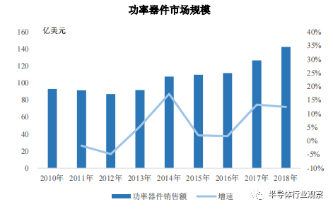
Figure 4: Power Device Market Size and Growth Rate
Note: Image source from Hu Silicon Industry prospectus
2.4. Sensors
Sensors (English name: transducer/sensor) are detection devices that can perceive the information being measured and can transform the perceived information into electrical signals or other required forms of output according to certain rules, meeting the requirements of information transmission, processing, storage, display, recording, and control. Sensors mainly include single material sensors, composite materials CMOS, and MEMS sensors. With the popularity of multi-camera smartphones, CMOS image sensors have rapidly grown; the new fingerprint recognition feature in smartphones has also increased the demand for sensors; the rapid development of autonomous driving technology has increased the demand for various types of sensors such as image sensors, LiDAR, and ultrasonic sensors.
The characteristics of sensors include miniaturization, digitization, intelligence, multifunctionality, systematization, and networking. They are the primary link for achieving automatic detection and automatic control. The existence and development of sensors have given objects tactile, taste, and olfactory sensations, bringing them to life. Generally, sensors can be classified into ten categories based on their basic sensing functions: thermal sensors, light-sensitive elements, gas-sensitive elements, force-sensitive elements, magnetic-sensitive elements, humidity-sensitive elements, sound-sensitive elements, radiation-sensitive elements, color-sensitive elements, and taste-sensitive elements.
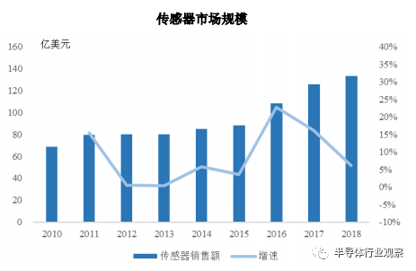
Figure 5: Sensor Market Size and Growth Rate
Note: Image source from Hu Silicon Industry prospectus
3. Understanding Semiconductors from the Perspective of the Industry Chain
From the perspective of the industry chain, the electronic information industry chain includes the upstream semiconductor industry represented by integrated circuits, the midstream electronic components and modules industry, and the downstream assembly and terminal application industry.
Upstream represented by integrated circuits: The main industry chain of integrated circuits consists of IC design, IC manufacturing, and IC packaging/testing. (The main bottleneck breakthrough relies on talent in investment and research.)
The midstream electronic components industry is experiencing further deepening of industrial division of labor, with module manufacturers producing whole modules by integrating numerous small components, then supplying them to downstream assembly factories. (The main bottleneck breakthrough relies on refined division of labor, company management models, and optimization and screening of upstream partner companies.)
The downstream assembly and terminal applications produce electronic products aimed at the market, with major application fields including smartphones, personal computers, industrial medical applications, and automotive electronics. (The main bottleneck breakthrough relies on market occupation and optimization screening of midstream and upstream partner companies.)
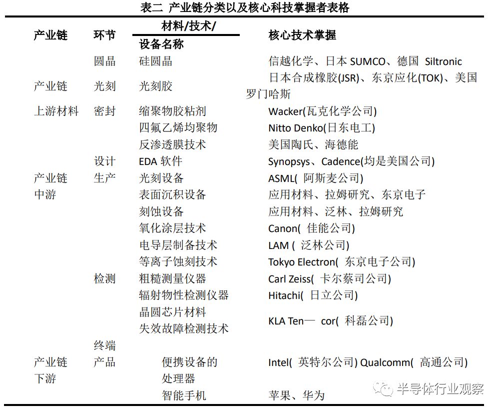
From the perspective of the entire semiconductor industry chain, the highest technical barriers exist in the upstream IP supply and IC design segments, followed by semiconductor equipment and wafer manufacturing. The packaging/testing industry has relatively lower barriers in the industry chain. The industry chain represents the value distribution chain, and the article will further analyze the semiconductor industry based on materials mastered by the author, dividing it into upstream, midstream, and downstream.
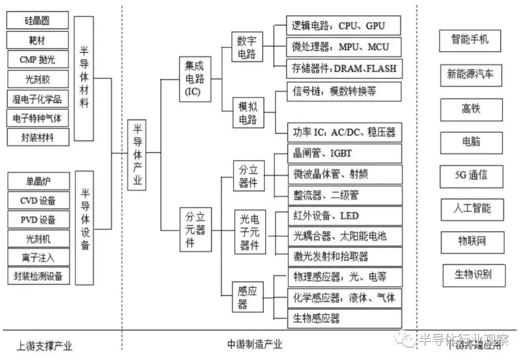
Figure 6: Semiconductor Industry Chain Classification
Note: Source from China National Knowledge Infrastructure
3.1. Upstream of the Industry Chain: Material Production and Equipment
Semiconductor materials can be divided into two major categories: wafer manufacturing materials and packaging materials. Among them, silicon wafers, gases, photomasks, and photoresists account for over 67% of the overall market size, with silicon and silicon-based materials accounting for about 32% of the semiconductor manufacturing materials market. Japan occupies more than half of the global semiconductor silicon material market share, while the US holds a monopoly in certain areas. Dow Chemical in the US holds over 90% of the market share for polishing materials used in manufacturing, while Cree in the US has a high monopoly in third-generation semiconductor materials such as silicon carbide and gallium nitride. Domestic semiconductor companies heavily rely on imports for materials, with few local material manufacturers, particularly for 12-inch large-size integrated circuit-grade silicon wafers, which still rely significantly on imports, mainly including Shanghai Xinsheng, Suzhou Ruihong, and Beijing Kehua. Shanghai Xinsheng Semiconductor has made breakthroughs in 12-inch wafer technology, but its monthly production capacity is only 70,000 to 100,000 wafers, with a small market share.
The semiconductor equipment market is highly monopolized, with core equipment in wafer manufacturing including photolithography machines, etching machines, and thin-film deposition equipment, accounting for about 30%, 25%, and 25% of the wafer manufacturing segment, respectively. In packaging equipment, the main equipment includes thinning machines, dicing machines, and packaging machines. Domestic semiconductor equipment companies are exhibiting rapid growth trends, but there is still a gap compared to companies in the US and Japan. US equipment companies account for as much as 56% of the global market share, while China only accounts for 3%. Among the top five global semiconductor equipment companies, US companies Applied Materials, Lam Research, and KLA dominate the market. Currently, China’s domestic semiconductor equipment industry shows characteristics such as low self-sufficiency rates and significant demand gaps. While low-end processes have achieved domestic substitution, high-end processes urgently need breakthroughs, with major manufacturers including North Huachuang, Zhongwei Semiconductor, and China Electronics Technology Equipment.
Leading IP suppliers like ARM and Fabless IC design leaders like Qualcomm allocate 30% and 20% of their annual revenue to R&D, respectively; leading semiconductor equipment companies like ASML and foundry leaders like TSMC allocate 11% and 8% of their annual revenue to R&D, respectively. In contrast, leading packaging/testing companies like ASE allocate only about 4% of their annual revenue to R&D. Compared to other segments in the semiconductor industry chain, the packaging/testing segment has relatively high barriers to capital investment, only lower than the wafer manufacturing segment, requiring significant capital investment for building factories and purchasing equipment. ASE’s average capital expenditure has accounted for 22.1% of the company’s revenue over the past three years.
3.2. Midstream of the Industry Chain: Device Production and Manufacturing
Semiconductor products mainly include two categories: integrated circuits (ICs, or chips) and semiconductor discrete devices (D-O-S). Integrated circuits/chips can be divided into digital circuits and analog circuits. Digital circuits can be further divided into microprocessors, logic circuits, and memory. Integrated circuits/chips refer to complex electronic systems that are “integrated” on a single semiconductor wafer through a series of specific planar manufacturing processes, connecting active devices like transistors and diodes with passive components like resistors and capacitors according to a specific circuit relationship, and are packaged in a protective shell. Representative devices include bipolar integrated circuits with types such as TTL, ECL, HTL, LST-TL, STTL, etc., and unipolar integrated circuits with types such as CMOS, NMOS, PMOS, etc.
Semiconductor discrete devices can be divided into discrete devices (diodes, transistors, etc.), optoelectronic devices, and sensor devices. Discrete devices refer to ordinary electronic components such as resistors, capacitors, and transistors, which are the smallest components without any integrated elements. Representative devices include semiconductor crystal diodes and semiconductor transistors. Optoelectronic devices refer to various functional devices made using semiconductor photoelectric (or electro-photon) conversion effects. Representative devices include light-emitting diodes (LEDs) and laser diodes (LD), photodetectors or photo-receivers, and solar cells. Sensor devices are essential components of sensors, capable of sensitively perceiving certain physical, chemical, or biological information and converting it into electrical information. Representative devices include thermistors, piezoresistors, photoresistors, force-sensitive resistors, magnetic-sensitive resistors, gas-sensitive electronics, and humidity-sensitive resistors.
In semiconductor products, integrated circuits/chips account for about 80%, while semiconductor discrete devices account for about 20%. Since most semiconductor products are integrated circuits/chips, the terms semiconductor and integrated circuits/chips are often used interchangeably. The upstream of the integrated circuit/chip industry chain mainly involves the raw materials and production equipment required for the manufacturing of integrated circuits/chips. The production processes of integrated circuits/chips mainly involve chip design, wafer processing, packaging, and testing. Integrated circuits/chips are primarily applied in downstream industries such as communication devices (including mobile phones), PCs/tablets, consumer electronics, and automotive electronics.
3.3. Downstream of the Industry Chain: Product Application and Sales
Gartner’s report indicates that the largest two fields in the finished product market are mobile and computing, reflecting the growth direction over the past year. The former is mainly driven by the smartphone and storage market, with sales increasing by 9.6% year-on-year, while the latter is affected by the decline in PC and tablet sales, with sales decreasing by 83% year-on-year. Research firm Gartner states that with the improvement of inventory conditions for memory, the Internet of Things (IoT), and other markets using Application-Specific Standard Products (ASSP), along with rising average selling prices (ASP), the global semiconductor market size is expected to grow by 9.2% in 2022, reaching $864.1 billion: the growth rate will exceed the 1.5% in 2021, sweeping away the previous gloom in the overall market, showing numerous development signs in the global semiconductor market.
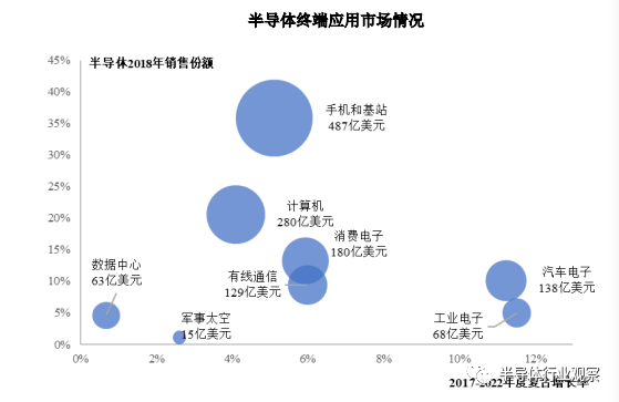
Figure 7: Semiconductor Terminal Application Market Situation
Note: Image source from Hu Silicon Industry prospectus
Gartner predicts that the fastest-growing semiconductor terminal application fields from 2017 to 2022 will be industrial electronics and automotive electronics, which will become the most important driving forces for growth in the global semiconductor industry in the coming years. The industrial electronics sector is expected to achieve a compound annual growth rate of 12%. As industries transition from scale to automation and intelligence, the deep integration of industry and information technology, as well as the transformation and upgrading of intelligent manufacturing, will drive the growth of industrial electronics demand. The automotive electronics sector is expected to have a compound annual growth rate of 11% from 2017 to 2022. The growth in automotive electronics mainly stems from the expansion of traditional vehicle electronic functions, the continuous maturation of autonomous driving technology, and the rapid growth of the electric vehicle industry. Various semiconductor products are required for vehicle systems such as ABS (Anti-lock Braking System), onboard radar, onboard image sensing systems, electronic stability programs, electronic suspension, electronic handbrakes, pressure sensors, accelerometers, gyroscopes, and flow sensors, greatly boosting the growth of automotive electronics products. With the popularization of electric vehicles and the continuous improvement of vehicle voltage and battery capacity standards, the demand for power management devices and discrete power devices will also increase accordingly.
Note: Some data in this article has been processed based on company official announcements, and all image sources are cited! Additionally, the companies mentioned in this article are introduced in sequence, and do not represent the author’s or any institution’s views, but merely a matter of stating order. Moreover, due to the author’s limited information, if there are any inappropriate introductions, the author hereby expresses apologies!


E课网(www.eecourse.com) is a professional integrated circuit education platform under Moore Elite, dedicated to the cultivation of high-quality integrated circuit professionals in the semiconductor industry. The platform is oriented towards the job demands of integrated circuit companies, providing a practical training platform that aligns with the corporate environment. Through online and offline training methods, it rapidly cultivates students to meet corporate needs.
E课网 has a mature training platform, a complete curriculum system, and a strong teaching faculty, planning a high-quality semiconductor course system of 168 courses, covering the entire integrated circuit industry chain, and has four offline training bases. To date, it has deeply trained a total of 15,367 people, directly supplying 4,476 professionals to the industry. It has established deep cooperative relationships with 143 universities and has held 240 special IC training sessions for enterprises.