Source: Comprehensive Semiconductor
Original Author: YuanYuanDeYuan
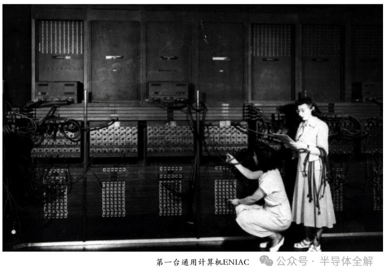
In February 1946, the world’s first electronic computer, ENIAC (Electronic Numerical Integrator And Computer), was born in the United States. It was a massive device weighing 30 tons, using 17,468 vacuum tubes, 7,000 resistors, and 10,000 capacitors, consuming 150 kilowatts of power.
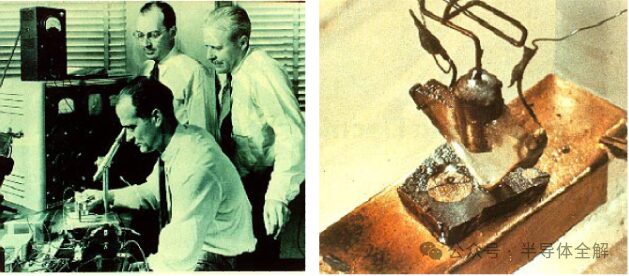
On December 23, 1947, Bell Labs in the United States manufactured the first transistor. The transistor had the main functions of vacuum tubes and overcame their drawbacks of large size, high power consumption, and fragility.
The Nobel Prize in Physics in 1956 was awarded to the three inventors of the transistor: John Bardeen, William Shockley, and Walter Brattain. After the invention of the transistor, the concept of integrated circuits based on semiconductors emerged quickly.
In 1952, Geoffrey Dummer, a scientist at the British Radar Research Laboratory, proposed at a conference that if discrete components in electronic circuits could be integrated onto a single semiconductor chip, the size of the electronic circuit would be greatly reduced, and reliability would improve. This was the initial concept of integrated circuits, made possible by the invention of the transistor.
The following image shows the three inventors of the transistor and the prototype of the world’s first transistor.
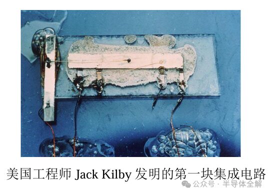
Between 1958 and 1959, Jack Kilby of Texas Instruments and Robert Noyce of Fairchild Semiconductor separately invented germanium and silicon integrated circuits, marking the beginning of the history of microelectronics.
Jack Kilby received the Nobel Prize in Physics in 2000 (Robert Noyce had passed away in 1990).
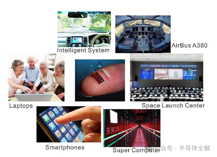
Integrated circuits are the cornerstone of modern information society, playing a vital role in various industries, such as televisions, computers, communications, artificial intelligence, virtual reality devices, etc.
2. Moore’s Law
On April 19, 1965, Gordon Moore, one of the founders of Intel and then Director of Research and Development at Fairchild Semiconductor, was invited to write an observational commentary for the 35th anniversary issue of Electronics Magazine titled: “Cramming More Components Onto Integrated Circuits.” In it, he predicted that the number of transistors integrated on semiconductor chips would double every year, which became known as Moore’s Law. In 1975, Moore revised this prediction at the IEEE International Electron Devices Meeting, changing “doubling every year” to “doubling every two years.” Later, David House, then Executive Chairman of Intel, updated this cycle to 18 months, considering factors such as the number of transistors and growth rates. The more accurate statement of Moore’s Law is: when prices remain unchanged, the number of components that can be accommodated on integrated circuits doubles every 18 to 24 months, and performance also doubles. For over 40 years, the number of transistors integrated on microprocessors has matched the predictions of Moore’s Law. The manufacturing technology of integrated circuits is one of the fastest-developing technologies in human technological history, with its cost-performance ratio improving by six orders of magnitude over the past 40 years.
In the semiconductor industry, Moore’s Law has been used to guide long-term research and development plans. Advances in microprocessor prices, memory capacities, sensors, and pixel sizes of digital cameras are closely related to Moore’s Law.
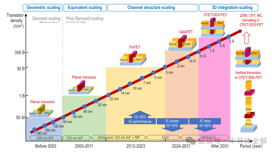
There are generally three methods to improve the performance of integrated circuits: reducing the feature size of individual transistors, increasing the size of the chip, and optimizing circuit structures.
Considering the trend towards miniaturization of electronic devices, reducing the feature size of individual transistors is the primary method for the development of integrated circuits. The reduction in transistor size can lower power consumption, increase the response speed of integrated circuits, and increase the number of transistors per unit area on the chip. The smallest feature size, also known as critical dimension (CD), can also be referred to as a node.
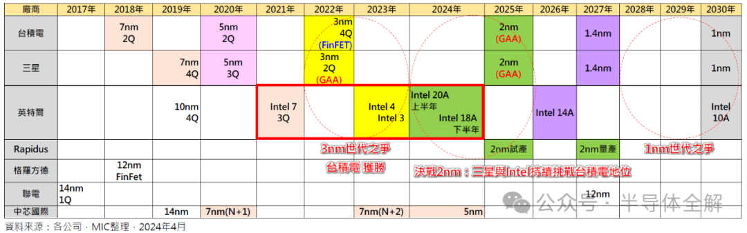
Currently, the semiconductor manufacturing industry continues to challenge the limits of Moore’s Law. The 3nm process has achieved mass production, the 2nm process is in the research and development stage, and the 1nm process has also been put on the agenda. In contrast, the established leader Intel has been unable to achieve breakthroughs in process technology and is even seeking TSMC for foundry services to gain a share of the global high-end chip market.
Moore’s Law is a statistical conjecture rather than a physical or natural law. To maintain Moore’s Law, the research and development capital required each year will grow exponentially, which is known as Moore’s Second Law. Additionally, as feature sizes approach physical limits, it will be difficult for technology nodes to advance at the rates predicted by Moore’s Law. The industry has proposed two paths: More Moore and More than Moore, to maintain the development of the semiconductor industry through new architectures or materials. The first is to follow Moore’s Law, focusing on the continuous scaling of transistors to improve performance, thereby further enhancing performance and reducing power consumption, i.e., More Moore. The second is to expand Moore’s Law, improving chip performance through circuit design, system algorithm optimization, or packaging technology, i.e., More than Moore.
3. Semiconductor Chip Manufacturing Technology
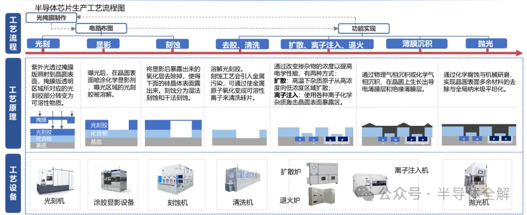
The manufacturing of integrated circuits involves nearly 800 physical and chemical processes, primarily consisting of five manufacturing stages: wafer preparation, chip manufacturing, chip testing, chip packaging, and acceptance testing.
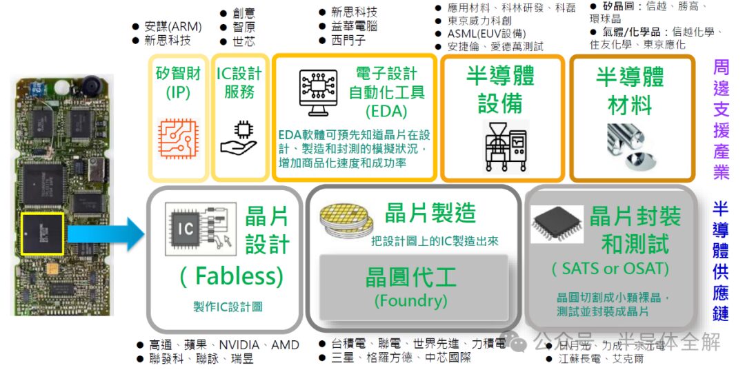
The production of semiconductor chips mainly involves three key stages: IC design, IC manufacturing, and IC packaging.
The core IC manufacturing stage is the process of transferring the chip circuit diagram from the mask to the silicon wafer and realizing the corresponding functions, which includes steps such as lithography, etching, ion implantation, thin film deposition, and chemical mechanical polishing.
The manufacturing of chips requires the use of lithography technology. Lithography is a photographic plate-making technology that uses a light-sensitive polymer (photoresist) as the main material, aiming to etch the complete integrated circuit pattern onto the wafer.
The word “Lithography” comes from the Greek words “lithos” meaning “stone” and “graphia” meaning “to write.” Therefore, the literal meaning of “lithography” is “writing on stone.” In the chip manufacturing process, the information of the integrated circuit is written into the photoresist.
The cost of lithography accounts for about one-third of the total chip manufacturing cost, and the time spent accounts for approximately 40-60% of the entire chip processing time, making it the most complex, expensive, and critical process in large-scale integrated circuit manufacturing.
Typically, the lithography process involves eight steps: gas phase base film formation, spin coating, soft baking, alignment exposure, post-bake, development, hard baking, and inspection.
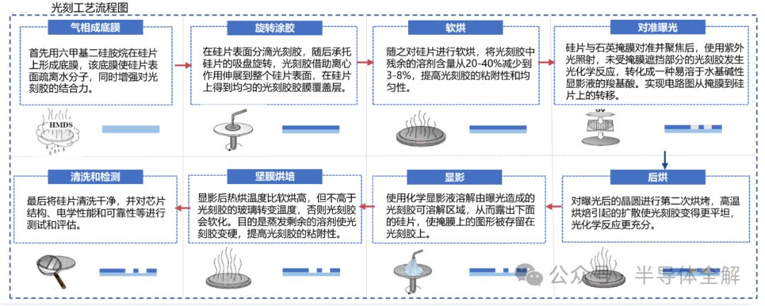
The main steps of the lithography process are as follows:
Pre-treatment: The cleaning of the wafer substrate is usually done with acetone to remove stains, followed by alcohol to eliminate acetone, and finally cleaned with deionized water (DI water) and blown dry with nitrogen.
Coating: A uniform layer of photoresist is applied to the surface of the wafer.
Soft Bake: The photoresist is baked to remove solvents and shape it.
Alignment Exposure: The pattern of the mask is projected onto the photoresist. Sometimes multiple exposures are needed on the same substrate, which requires precise alignment each time to ensure that multiple lithographies do not interfere with each other.
Post Bake: The purpose is to reduce standing wave effects and make the exposed part of the photoresist easily soluble in the developer (positive photoresist).
Development: Development is meant to remove the altered photoresist to form a sample surface identical to the mask plate.
Hard Baking: There are four purposes: first, to completely evaporate the solvent in the photoresist to avoid contaminating the subsequent ion implantation environment; second, to harden the film to protect the underlying wafer during ion implantation or etching; third, to further enhance the adhesion between the photoresist and the silicon wafer surface; and fourth, to further reduce standing wave effects.
Etching Doping: Using the exposed sample pattern, etching can form the desired sample, a process also known as pattern transfer.
Stripping: The residual photoresist is cleaned off, and baking is also required to form a solid finished product.
Typically, it takes 25 to 40 repeated exposures and etchings to replicate an integrated circuit pattern containing millions of transistors and corresponding wires onto a wafer.
Since the development of integrated circuits, the circuit integration level has increased by six orders of magnitude, primarily due to advances in lithography technology. As the device and circuit feature sizes continue to shrink, lithography processes have become the major bottleneck for further development of microelectronics technology.
4. Development of Chip Performance
Lithography technology is crucial because the lithography process determines the size of the transistors!
Transistors are the basic units of chips, and a silicon wafer consists of thousands, tens of thousands, or even hundreds of millions of transistors.
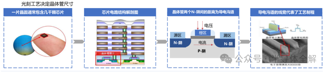
As shown in the image above, when a voltage is applied between the gate and the substrate of the transistor, current can flow from the source area to the drain area, forming an electrical signal, and the distance between the two N-wells corresponding to the source and drain areas is the length of the conductive channel, which is the size of the transistor, i.e., the line width, commonly referred to as the chip process.
Since electrons in transistors typically operate at saturation speed, the speed of information transmission is determined by the length of the conductive channel. The shorter the conductive channel of the transistor, the faster the signal transmission speed, meaning that more information can be processed by the chip in a given time; at the same time, there are also more transistors per unit area on the chip, which correspondingly reduces costs.
Therefore, the smaller the transistor line width indicator, the better the chip performance, indicating a gradual decrease in the technical requirements for chip processes, while the lithography process determines the size of the transistors and the advancement of process technology nodes.
The following image shows the structure of a transistor and the roadmap of line width development:
5. Structure of Lithography Equipment
Lithography technology is essentially the pattern transfer technology for IC chip manufacturing. This process of image transfer includes transferring the graphics from the design drawings to the mask substrate, then transferring the graphics from the mask plate to the photoresist on the wafer surface, and finally transferring the photoresist graphics on the wafer surface to the chip. The entire pattern transfer process involves many types of lithography machines.
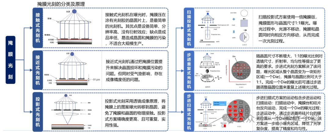
Based on the working principle, lithography machines can be categorized into mask lithography and maskless lithography, depending on whether a mask is used during exposure. Among them, mask lithography includes contact lithography machines, proximity lithography machines, and projection lithography machines; maskless lithography includes laser direct-write lithography machines, nanoimprint lithography machines, etc. The specific classification is shown in the image below.
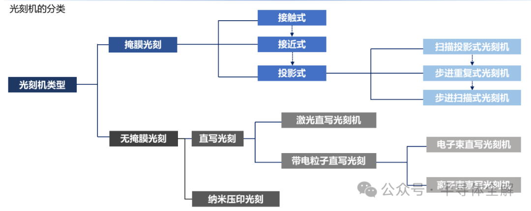
According to the positional relationship between the mask and the substrate during exposure, mask lithography can be divided into contact, proximity, and projection lithography. Among them, in projection lithography, based on the movement method of the mask and wafer during exposure, it can be further subdivided into scanning projection lithography machines, step-and-repeat lithography machines, and step-and-scan lithography machines.
Currently, ASML remains the industry leader in the mid-to-high-end lithography machine market, with a market share of over 70%. In comparison, Nikon has a significant price advantage among similar products, but its reputation in the industry is average, with a global market share of only about 10%, making it difficult to compete.
In recent years, ASML and its three major shareholders—Intel, Samsung, and TSMC—have formed a community of interest, striving to continuously challenge and achieve Moore’s Law.
It is worth noting that ASML places great emphasis on research and development investment, even during periods of loss, it has not reduced R&D costs, fundamentally ensuring its foresight and continuity.
Projection lithography machines mainly consist of light sources, illumination systems, mask stages, projection optics, and wafer control systems, as shown in the image below.

(1) Light Source: The light source system is the core of lithography equipment. The wavelength of the light source determines the process capability, and the technical progress of lithography machines is also a process of continuously shortening wavelengths.
The light source provides stable frequency and energy light for the lithography machine, and the power of the light source determines the production capacity of the lithography machine. Cymer is one of the important suppliers of light sources for lithography machines, having launched a series of products, including Krypton Fluoride (KrF) light sources, Argon Fluoride (ArF) light sources, and extreme ultraviolet light sources.
The shorter the wavelength of the light source, the smaller the transistor line width, and the stronger the chip performance. The light beam emitted by the light source passes through the illumination system, then through the mask, and is projected by the projection optics system onto the surface of the silicon wafer.
(2) Illumination System: The illumination system, as one of the core components of the lithography machine, is responsible for shaping and homogenizing the light beam emitted by the light source to illuminate the mask surface, and then the projection optics system replicates the pattern on the mask surface onto the silicon wafer.
The light path of the illumination system: The light from the light source goes through beam expansion, collimation, and transmission before entering the optical pupil shaping unit, and then passes through the illumination homogenization unit to achieve a specific distribution of the illumination light field. The scanning slit is used to determine the exposure field size and center position, control the exposure dose, and synchronize the scanning exposure with the mask stage and wafer stage.
The relay lens group is located between the scanning slit and the mask and is responsible for relaying the illumination light field on the scanning slit to the mask surface.
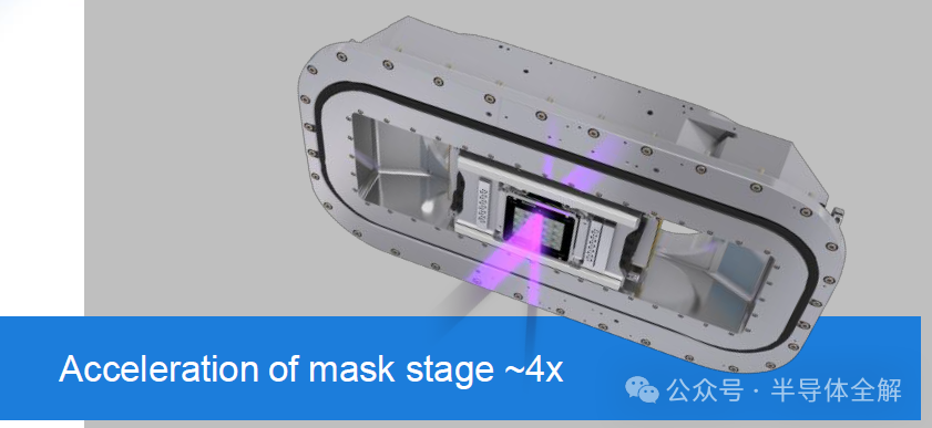
(3) Mask Stage: The mask stage is where the mask plate is placed and can be adjusted in multiple degrees of freedom. In the step-and-scan exposure mode, it works with the wafer stage to achieve extremely high precision synchronization of the mask and wafer.
(4) Projection Optics: The projection optics is the core component of the lithography machine, projecting the mask pattern onto the wafer without distortion. Its imaging quality requirements are extremely strict, usually requiring wavefront aberration and distortion to be within about 1nm.
The resolution R of the lithography machine is related to the wavelength λ of the light source and the numerical aperture NA, as expressed by the formula.
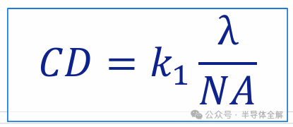
In the formula, k1 is the process factor. As the feature sizes of integrated circuits continue to shrink, the resolution of lithography machines continues to improve, and projection optics are also developing towards larger NA and shorter wavelengths.
It is worth mentioning that the higher-end lithography machines encounter increasingly complex optical problems, and only through deeper optical research can the overall performance of the equipment be improved.
Light is a form of electromagnetic wave, so it exhibits wave-particle duality.
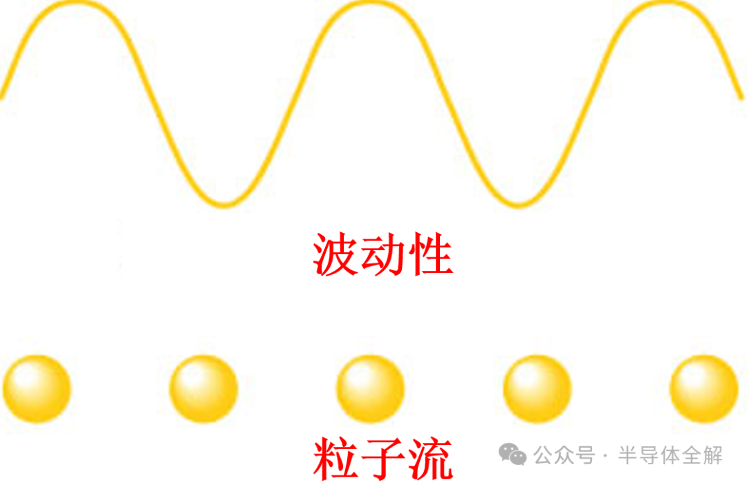
During the propagation of light, it can interfere with itself, either reinforcing or weakening each other:
Optical lenses during projection can experience spherical aberration, coma, defocus, field curvature, chromatic aberration, and other issues due to factors such as lens structure and light wavelength. As the numerical aperture of lithography machines increases, resolution decreases. To etch the finest possible lines, the wavefront aberration RMS across the entire field of view during the actual operation of the objective must be less than 0.07λ, with image plane curvature requirements of less than several tens of nanometers, and distortion not exceeding a few nanometers. Based on different aberrations and chromatic aberrations, lithography processes impose higher requirements on the production of projection optics.

Due to issues such as spherical aberration and chromatic aberration in single projection optics, it is necessary to use combined projection optics for correction in practical applications. As the numerical aperture increases, resolution reaches the diffraction limit, thus requiring greater precision in aberration correction, including extreme requirements for environmental control, compensation for aberrations of cold lenses/hot lenses, and lens surface flatness.
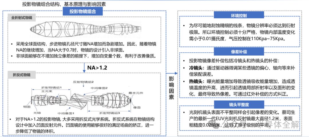
The image below shows the development of 193nm projection optics, with resolution improving from 130nm to 45nm.
To achieve high NA, starting from the StarlithTM 1100 model, projection optics began to use aspherical lenses, and from the StarlithTM 1700i model, immersion and reflective structures began to be adopted.

The development history of projection optics has mainly gone through the following forms: refractive, refractive + aspherical elements, refractive + aspherical elements + immersion, reflective + aspherical elements + immersion.
The limit of numerical aperture NA for refractive global surface structure is about 0.75, which can be increased to around 0.9 by adding aspherical elements. To further increase NA in the 193nm band, an immersion structure must be adopted, which involves immersing the image plane in deionized water.
Immersion refractive can achieve NA above 1.0, while immersion reflective can achieve NA 1.35.

To more finely control the wavefront of projection optics, the FlexWave system has been proposed, as shown in the image.
The FlexWave system includes an optical element located at the pupil plane, with a series of independent conduction and resistance structures arranged on it. These structures are tiny and do not obstruct or scatter the beam, affecting the imaging of the optics. By controlling the current of these conduction and resistance structures, specific areas of the optical element can be heated, allowing for a controllable temperature distribution to compensate for aberrations.
When FlexWave operates, it requires parallel cooling of the element to ensure that the temperature distribution on the FlexWave optical element remains stable and constant, while ensuring that its heat does not interfere with surrounding optical elements.
(5) Wafer Control System: The wafer control system loads, aligns, steps, scans, and unloads the wafer during the exposure process of the lithography machine, which is an extremely precise mechanical system.
6. Conclusion:
The complexity of lithography machines can be considered the pinnacle of human technology. On one hand, the manufacture of lithography machines is an extremely complex engineering field interwoven with multiple disciplines, integrating the wisdom of the world’s top engineers and scientists in precision optics, precision kinematics, high-precision microenvironment control, algorithms, microelectronics, and precision measurement and control.
On the other hand, lithography machines are a complete nanotechnology industrial system. To produce chips with nanometer-level precision, the underlying light source system, optical lens system, precision motion and environmental control systems, measurement systems, focusing systems, and alignment systems must all achieve nanometer-level precision and be highly integrated and coordinated. The technological iteration achievements of each subsystem contain the most cutting-edge technologies in that field.
It is no exaggeration to say that lithography machines are the pinnacle of human industrial civilization and the crown jewel of modern industrial systems.
References:
(1) Xu Xiangru, Research on the Image Quality Compensation Strategy and Polarization Aberration of High Numerical Aperture Projection Lithography Objective[D].
(2) Li Jing, Research on Wavefront Aberration Detection Technology of High NA Projection Lithography Objective[D].
(3) Hua Fu Securities, Deep Report on the Lithography Machine Industry: Gathering Stars to Illuminate the Crown Jewel[C].
(4) Minsheng Securities, Deep Report on the Mask Industry: The Lithography Blueprint Urgently Needs Breakthroughs, Domestic Substitution Has Great Potential[C].
(5) Shang Hongbo, Research on Optical Design and Aberration Compensation of Immersion Lithography Projection Objective[D].
(6) Rui Dawei, Research on Optical Design and Compensation Strategies of Lithography Illumination Systems[D].
(7) Xu Weicai, Optical Design and Image Quality Compensation of Projection Lithography Objectives[D].
(8) Zhou Zelong, Research on Polarization Aberration of Projection Lithography Objectives[D].
(9) Zhao Lei, Research on Image Quality Compensation Strategy and Compensation Technology of Projection Lithography Objectives[D].
END
The content is reprinted and only represents the author’s views
It does not represent the position of the Semiconductor Institute of the Chinese Academy of Sciences
Editor: Schrödinger’s Cat
Proofreader: Six Dollar Fish
Submission Email: [email protected]