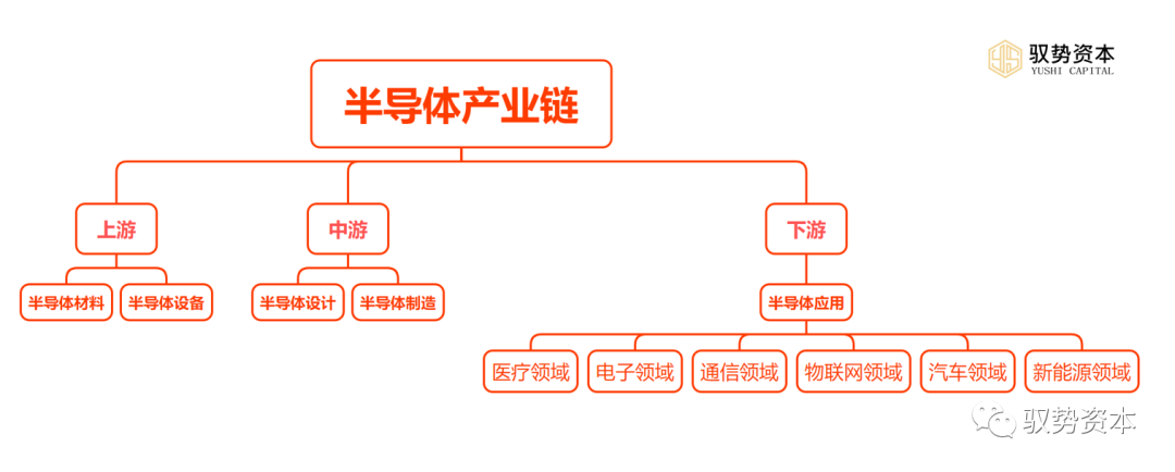
The most comprehensive semiconductor industry chain is divided into upstream, midstream, and downstream. The upstream includes semiconductor materials and semiconductor equipment, the midstream includes semiconductor design and semiconductor manufacturing, while the downstream involves the application fields of semiconductors.
1. Upstream of the Semiconductor Industry Chain
1.1 Semiconductor Materials
Semiconductor materials can be divided into front-end wafer manufacturing materials and back-end packaging materials. The specific classification is referenced in the following mind map:
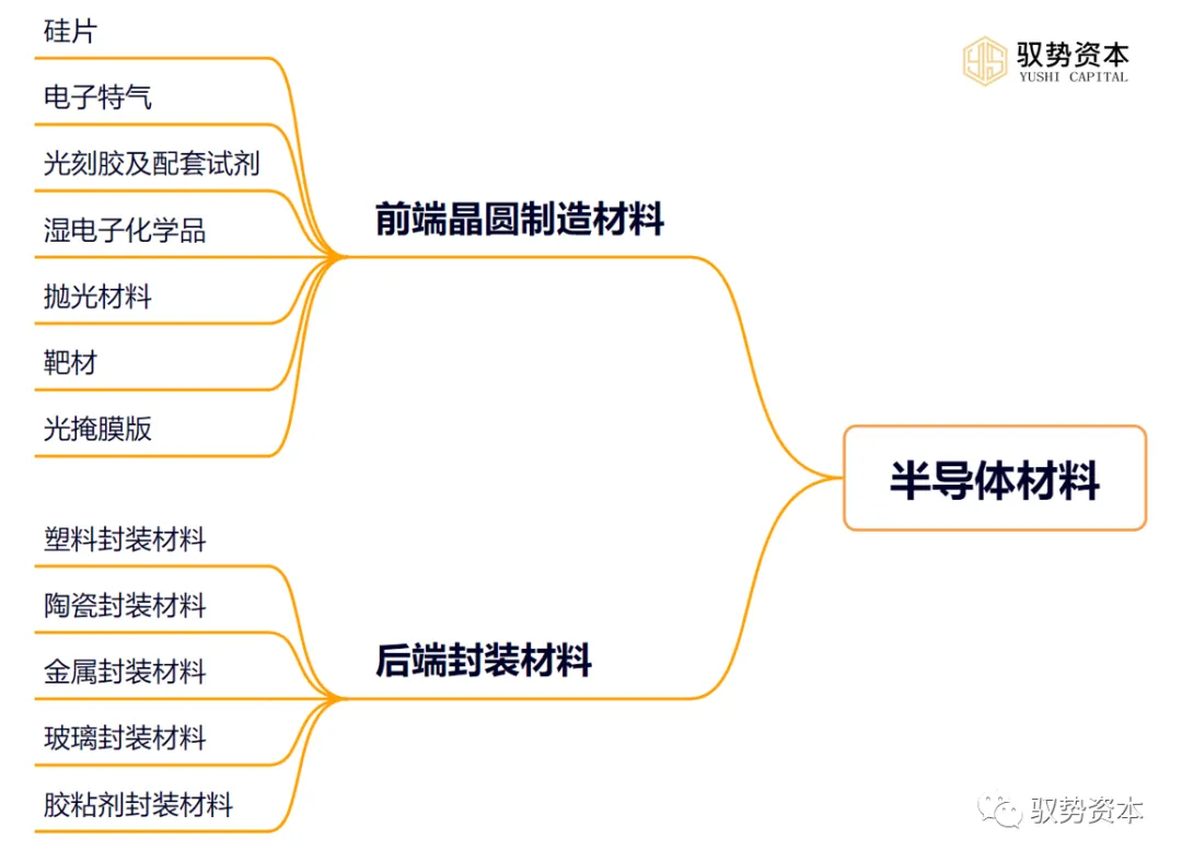
The front-end wafer manufacturing materials mainly include the following types: (1) Silicon Wafers: Silicon wafers are one of the most important materials in wafer manufacturing, accounting for about one-third of all wafer manufacturing materials. They are a type of high-purity single-crystal silicon with excellent physical and chemical properties, serving as the basic material for integrated circuits and semiconductor devices.
(2) Electronic Special Gases: Electronic special gases are essential materials required for manufacturing integrated circuits and semiconductor devices, mainly including high-purity nitrogen, hydrogen, oxygen, argon, etc. These gases are widely used in semiconductor manufacturing processes such as chemical vapor deposition, epitaxial growth, and ion implantation.
(3) Photoresist and Supporting Reagents: Photoresist is a photosensitive material used in photolithography processes, which can either transmit or block light beams, thereby transferring circuit patterns onto silicon wafers. Supporting reagents include developers, fixers, etc., used for processing and cleaning photoresist.
(4) Wet Electronic Chemicals: Wet electronic chemicals are liquid chemicals used in processes such as chemical etching and cleaning, including acids, bases, organic solvents, etc.
(5) Polishing Materials: Polishing materials are used for surface treatment of silicon wafers to achieve a highly smooth and shiny surface. Common polishing materials include cerium oxide, aluminum oxide, etc.
(6) Target Materials: Target materials are used to prepare thin film materials, such as tungsten, copper, etc. In the preparation process, the target material is heated to a molten state and then sputtered onto the silicon wafer by an ion beam, forming the required thin film.
(7) Photomasks: Photomasks are optical masks used to transfer circuit patterns onto silicon wafers, made from materials with different optical properties.
The back-end packaging materials mainly include the following types:
(1) Plastic Packaging Materials:Plastic packaging is a common packaging method, mainly using epoxy resin, thermosetting plastics, polyimide, etc. These materials have excellent electrical insulation properties, high-temperature resistance, and chemical corrosion resistance, while being cost-effective, thus widely used in back-end packaging.
(2) Ceramic Packaging Materials: Ceramic packaging materials have excellent thermal conductivity, electrical insulation, and corrosion resistance, making them widely used in high-reliability, high-temperature, and high-speed electronic device packaging. Common ceramic packaging materials include alumina, aluminum nitride, silicon nitride, etc.
(3) Metal Packaging Materials: Metal packaging materials have excellent thermal and electrical properties, thus widely used in high-reliability, high-temperature, and high-speed electronic device packaging. Common metal packaging materials include aluminum, copper, stainless steel, etc.
(4) Glass Packaging Materials: Glass packaging materials have excellent sealing and electrical insulation properties, thus widely used in high-reliability, low-cost electronic device packaging. Common glass packaging materials include borosilicate glass, silicate glass, etc.
(5) Adhesive Packaging Materials: Adhesive packaging materials are mainly used to fix the chip and the lead frame to the substrate while protecting the chip and lead frame from mechanical shocks and chemical corrosion. Common adhesive packaging materials include epoxy resin adhesive, polyimide adhesive, etc.
1.2 Semiconductor Equipment
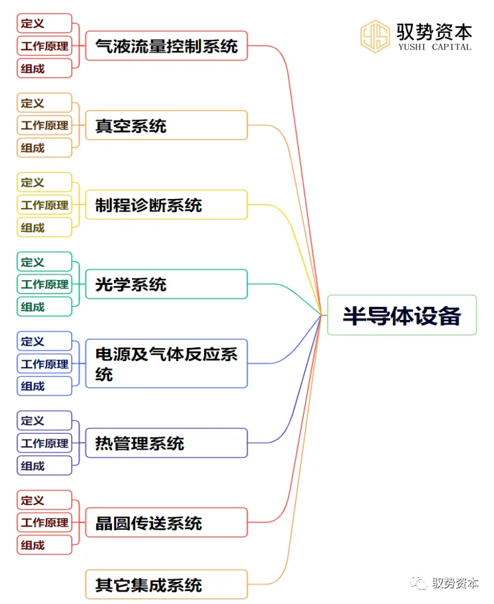
Semiconductor equipment mainly includes gas-liquid flow control systems, vacuum systems, process diagnostic systems, optical systems, power and gas reaction systems, thermal management systems, wafer transport systems, and other integrated systems. The specific content is referenced in the following mind map:
1) Gas-Liquid Flow Control System: The gas-liquid flow control system in semiconductor equipment is a system that precisely controls the flow rate of gases and liquids. Its working principle involves measuring parameters such as pressure difference, temperature, and density of fluids passing through a pipe, and based on the properties of the fluid, such as viscosity and compressibility, it calculates the flow rate through mathematical operations. Then, it compares the preset flow rate with the actual flow rate and adjusts the opening of valves or pumps accordingly, thus achieving precise flow control. Additionally, the gas-liquid flow control system can also monitor and control parameters such as temperature, pressure, and viscosity to ensure stability and reliability during the semiconductor manufacturing process. This system mainly includes flow meters, valves, pumps, pressure gauges, filters, flow controllers, sensors, electronic controllers, etc.
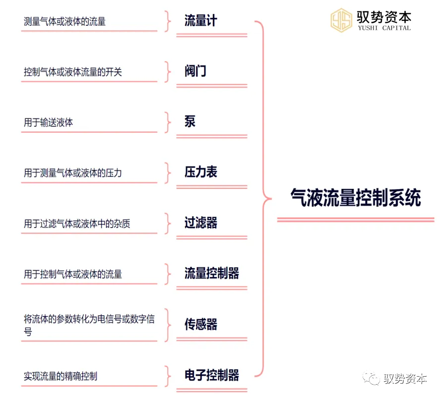
1) Flow Meter: Measures the flow rate of gases or liquids, typically using electromagnetic flow meters, ultrasonic flow meters, or thermal flow meters. These flow meters can convert the flow rate of fluids into electrical or digital signals for further processing and control by electronic controllers.2) Valves: Control the opening and closing of gas or liquid flow, typically using ball valves, gate valves, or needle valves. These valves can adjust the fluid flow based on commands from electronic controllers, thus achieving precise flow control.3) Pumps: Used for transporting liquids, typically using centrifugal pumps, piston pumps, or diaphragm pumps. These pumps can transport liquids from lower to higher positions to ensure stable and reliable liquid flow.4) Pressure Gauges: Used to measure the pressure of gases or liquids, typically using spring pressure gauges or digital pressure gauges. These pressure gauges can convert pressure into electrical or digital signals for further processing and control by electronic controllers.5) Filters: Used to filter impurities from gases or liquids, typically using mechanical filters, activated carbon filters, or ultrafiltration filters. These filters can remove impurities from fluids to ensure cleanliness and quality.6) Flow Controllers: Used to control the flow rate of gases or liquids, typically using electronic or mechanical flow controllers. These flow controllers can compare the preset flow rate with the actual flow rate and adjust the opening of valves or pumps accordingly, thus achieving precise flow control.7) Sensors: Used to measure parameters such as temperature, pressure, and viscosity of fluids and convert these parameters into electrical or digital signals for further processing and control by electronic controllers.8) Electronic Controllers: Compare the preset flow rate with the actual flow rate and adjust the opening of valves or pumps accordingly, thus achieving precise flow control. Additionally, electronic controllers can also monitor and control parameters such as temperature, pressure, and viscosity to ensure stability and reliability during the semiconductor manufacturing process.
(2) Vacuum System: The vacuum system in semiconductor equipment is a subsystem used to maintain and control the vacuum level within the manufacturing process. Its working principle mainly involves using vacuum pumps to extract air from the vacuum chamber, reducing its internal pressure below atmospheric pressure. Specifically, the vacuum pump removes air from the vacuum chamber and discharges it into the atmosphere through specialized piping. To maintain the desired vacuum level, the vacuum pump adjusts the pumping speed according to the actual pressure. At the same time, relevant measuring instruments monitor and display the pressure inside the vacuum chamber in real-time, ensuring it remains stable within the preset range. This system mainly includes vacuum chambers, vacuum pumps, vacuum measuring instruments, vacuum pipelines, valves, and leak prevention devices.
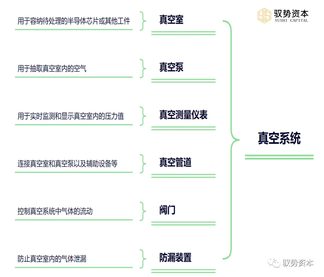
1) Vacuum Chamber: This is the core part of the vacuum system, used to hold the semiconductor chips or other workpieces to be processed. Vacuum chambers are generally made of high-pressure resistant and corrosion-resistant materials, such as stainless steel or titanium alloys.2) Vacuum Pump: Used to extract air from the vacuum chamber and maintain the required vacuum level. Depending on actual needs, different types of equipment, such as mechanical pumps, molecular pumps, or dry pumps, can be selected.3) Vacuum Measuring Instruments: Used to monitor and display the pressure inside the vacuum chamber in real-time, ensuring the stability of the vacuum level.4) Vacuum Pipelines: Connect the vacuum chamber and vacuum pump, as well as various valves and auxiliary devices.5) Valves: Control the flow of gases in the vacuum system, such as vacuum valves, pressure valves, etc.6) Leak Prevention Devices: Prevent gas leakage from the vacuum chamber, ensuring the system’s sealing properties.
(3) Process Diagnostic System: The process diagnostic system in semiconductor equipment is a key subsystem used to monitor and evaluate various parameters during the semiconductor manufacturing process in real-time. Its working principle mainly involves collecting and analyzing equipment operating data to determine process status. Specifically, data collectors obtain real-time data from the equipment and transmit it to data processors for processing and analysis. By applying mathematical models and algorithms, data processors extract key parameters related to process performance and store them in a database. Diagnosis algorithms evaluate the current process status based on the data in the database and predetermined process standards. Once a deviation from the preset range is detected, the alarm system immediately triggers and notifies relevant personnel to take corrective measures. At the same time, controllers and actuators automatically adjust process parameters based on the analysis results to ensure the equipment operates in optimal conditions. This system mainly includes data collectors, data processors, databases, diagnostic algorithms, user interfaces, alarm systems, controllers, and actuators.
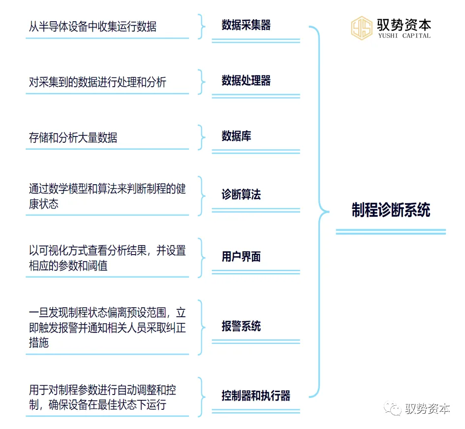
1) Data Collector: Used to collect operating data from semiconductor equipment, such as temperature, pressure, current, voltage, etc.2) Data Processor: Processes and analyzes the collected data to extract key information regarding process status.3) Database: Stores and analyzes large amounts of data to provide historical trends and comparative information about process performance.4) Diagnostic Algorithms: Based on the data in the database and predetermined process standards, assess the health status of the process using mathematical models and algorithms.5) User Interface: Allows engineers and technicians to visualize the analysis results and set corresponding parameters and thresholds.6) Alarm System: Triggers alarms and notifies relevant personnel to take corrective measures once deviations from preset ranges are detected.7) Controllers and Actuators: Automatically adjust and control process parameters to ensure that the equipment operates in optimal conditions.
(4) Optical System: The optical system in semiconductor equipment is a subsystem that uses optical principles and techniques for precise analysis and control of semiconductor materials and devices. Its working principle mainly involves using light interference, diffraction, scattering, and other principles for precise analysis and control of semiconductor materials and devices. Specifically, light emitted from a light source is guided through an optical path system to illuminate the semiconductor material or device to be analyzed. Reflected or transmitted light is received by a detector and converted into electrical signals, which are then digitally processed and analyzed through an image processing system to extract information about the semiconductor materials and devices. The control system precisely controls the optical system according to process requirements, ensuring the accuracy and stability of the entire analysis process. This system mainly includes light sources, optical path systems, detectors, image processing systems, control systems, auxiliary equipment, etc.
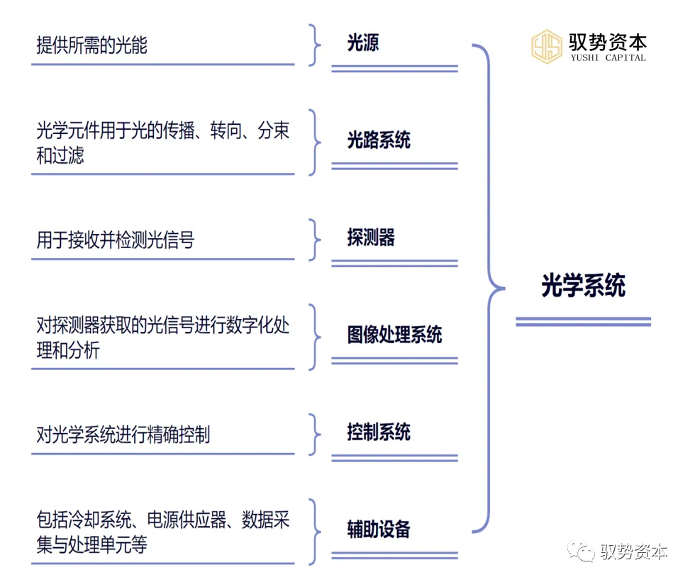
1) Light Source: Provides the required light energy, including lasers, ultraviolet light, visible light, etc., of various wavelengths and energies.2) Optical Path System: Includes optical components such as mirrors, refractors, beam splitters, filters, etc., used for light propagation, steering, splitting, and filtering.3) Detector: Used to receive and detect light signals, including photomultiplier tubes, CCD cameras, CMOS sensors, etc.4) Image Processing System: Digitally processes and analyzes the light signals obtained by the detector to extract information about the semiconductor materials and devices.5) Control System: Precisely controls the optical system according to process requirements, enabling automated or semi-automated operation.6) Auxiliary Equipment: Includes cooling systems, power supplies, data acquisition, and processing units, etc.
(5) Power and Gas Reaction System: The power and gas reaction system in semiconductor equipment is a comprehensive subsystem involving the collaborative operation of multiple components. These components work together to provide necessary support and control for power supply, gas supply, chemical reactions, and physical deposition processes during semiconductor manufacturing. Its working principle mainly involves supplying electrical energy through the power supply to drive chemical reactions and physical deposition processes in the reaction chamber. Specifically, the power supply outputs specific voltage and current based on the equipment’s requirements, providing energy for chemical reactions in the reaction chamber. At the same time, the gas supply system ensures the purity and pressure stability of the gases in the reaction chamber. When the reaction is complete, the exhaust gas treatment system filters and processes the exhaust gas before discharge. The control system precisely controls the entire process to ensure stability and repeatability of the reactions. This system mainly includes power supplies, gas supply systems, reaction chambers, exhaust gas treatment systems, control systems, auxiliary equipment, etc.
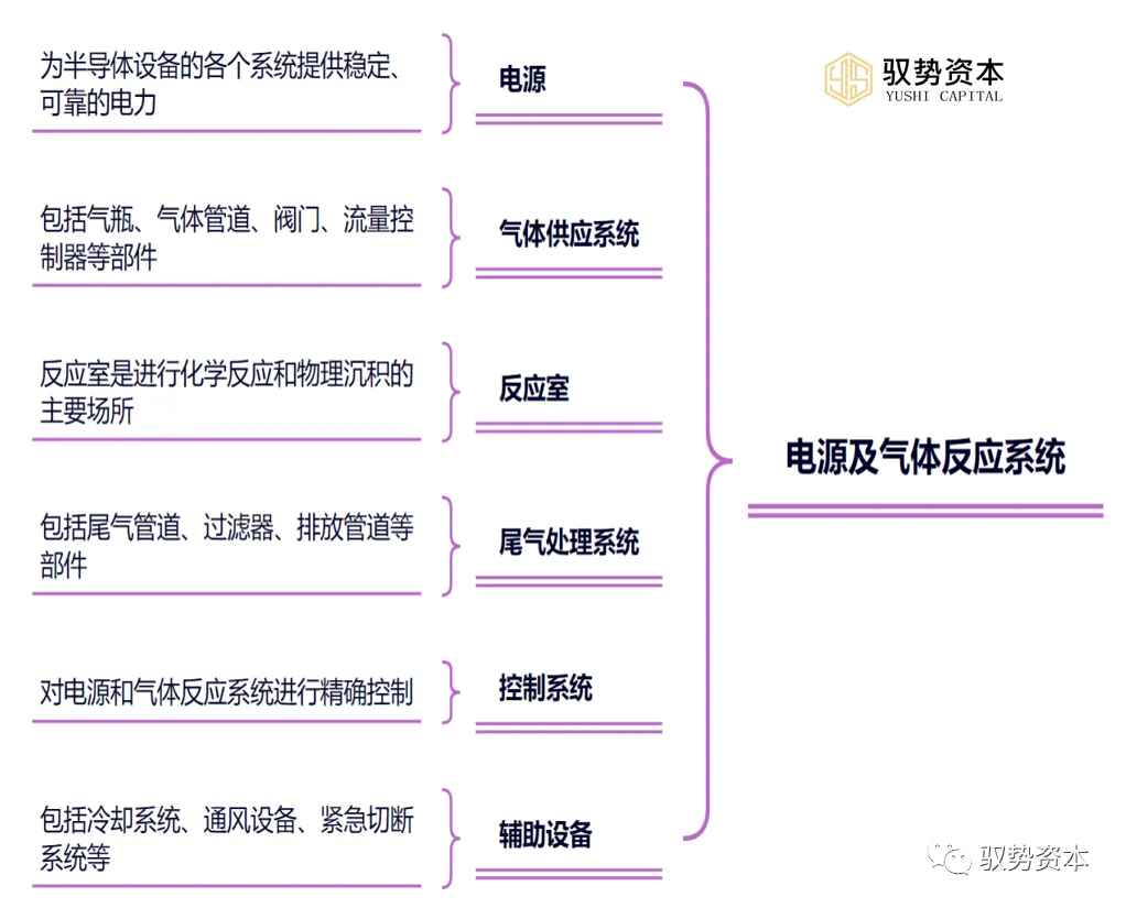
1) Power Supply: Provides stable and reliable power to various systems of semiconductor equipment. The output voltage and current of the power supply need to be configured according to the specific requirements of the equipment.2) Gas Supply System: Includes gas cylinders, gas pipelines, valves, flow controllers, etc., used to supply reaction gases and inert gases, maintaining the purity and pressure stability of gases within the equipment.3) Reaction Chamber: The reaction chamber is the main site for chemical reactions and physical deposition, typically made of stainless steel or other corrosion-resistant materials.4) Exhaust Gas Treatment System: Includes exhaust gas pipelines, filters, discharge pipelines, etc., used to process exhaust gases generated after reactions, ensuring compliance with environmental protection requirements.5) Control System: Precisely controls the power supply and gas reaction system, enabling automated or semi-automated operations. The control system typically consists of various sensors, controllers, and actuators.6) Auxiliary Equipment: Includes cooling systems, ventilation equipment, emergency shutdown systems, etc., to ensure the normal operation and safety of the power and gas reaction system.
(6) Thermal Management System: The thermal management system in semiconductor equipment is a key subsystem used to control and maintain stable internal temperatures of the equipment. Its working principle involves precisely controlling the operation of heaters and cooling systems through a control system to maintain stable internal temperatures. Specifically, temperature sensors monitor the internal temperature of the equipment in real-time, feeding back temperature signals to the control system. The control system adjusts the operation of heaters and cooling systems based on the difference between the set temperature and the actual temperature, redistributing heat within the equipment. If the internal temperature is too high, the control system activates the cooling system to dissipate excess heat; if the internal temperature is too low, the control system adjusts the power of the heater to generate an appropriate amount of heat to maintain temperature stability. Through this precise temperature control, the thermal management system ensures that the performance and yield of semiconductor equipment are not affected by temperature fluctuations. This system mainly includes heaters, cooling systems, temperature sensors, control systems, insulation materials, airflow control systems, auxiliary equipment, etc.
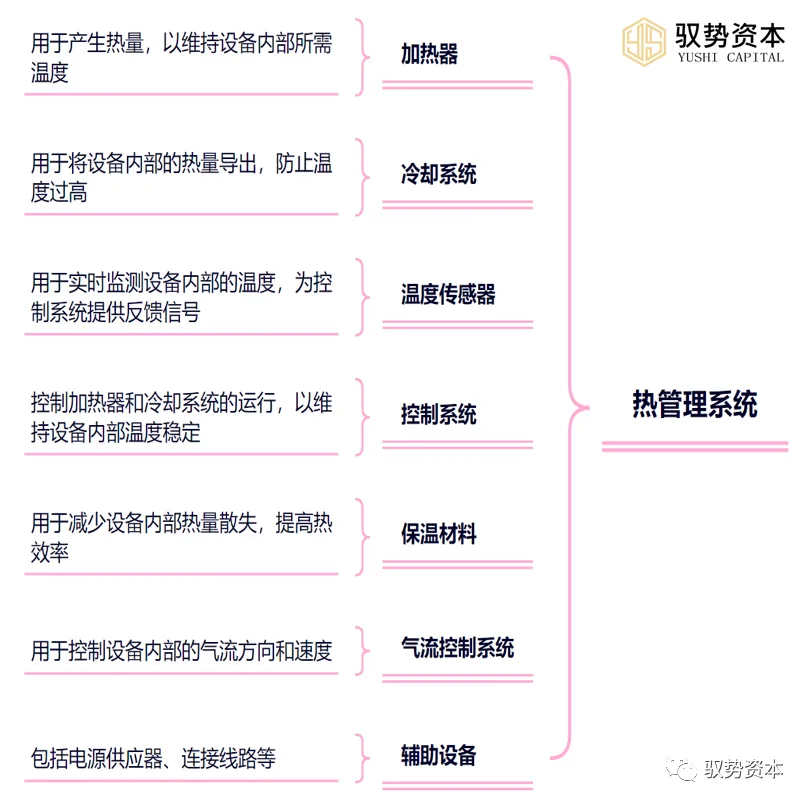
1) Heater: Used to generate heat to maintain the required internal temperature of the equipment. Heaters can be of various types, including resistive, inductive, or infrared.2) Cooling System: Used to dissipate heat from within the equipment, preventing excessive temperatures. Cooling systems typically include radiators, fans, water cooling systems, etc.3) Temperature Sensors: Used to monitor the internal temperature of the equipment in real-time, providing feedback signals to the control system.4) Control System: Controls the operation of heaters and cooling systems based on feedback signals from temperature sensors to maintain stable internal temperatures. The control system typically consists of controllers, actuators, etc.5) Insulation Materials: Used to reduce heat loss within the equipment, improving thermal efficiency. Insulation materials are usually made from highly thermally conductive materials, such as graphene, nano-insulation materials, etc.6) Airflow Control System: Used to control the direction and speed of airflow within the equipment, ensuring uniform temperature distribution.7) Auxiliary Equipment: Includes power supplies, connecting lines, etc., providing power and support for the entire thermal management system.
(7) Wafer Transport System: The wafer transport system in semiconductor equipment is a key subsystem used for the rapid and accurate transport of wafers between various process steps. Its working principle involves precisely controlling devices such as robotic arms, conveyor belts, and robots to achieve fast and accurate transport of wafers between different process steps. During transport, the wafers are accurately positioned and secured on the transport device to ensure their stability and safety during various process steps. The control system plans the optimal transport path and speed based on process flow and device parameters, while monitoring the operating status of the equipment and the positioning accuracy of the wafers. The communication system ensures smooth information exchange between devices to promptly adjust process parameters and control commands. The power supply and signal transmission devices provide the necessary power and signal transmission for the entire system, ensuring stable operation of the equipment. This system mainly includes transport devices, positioning systems, control systems, communication systems, power supply and signal transmission devices, auxiliary equipment, etc.
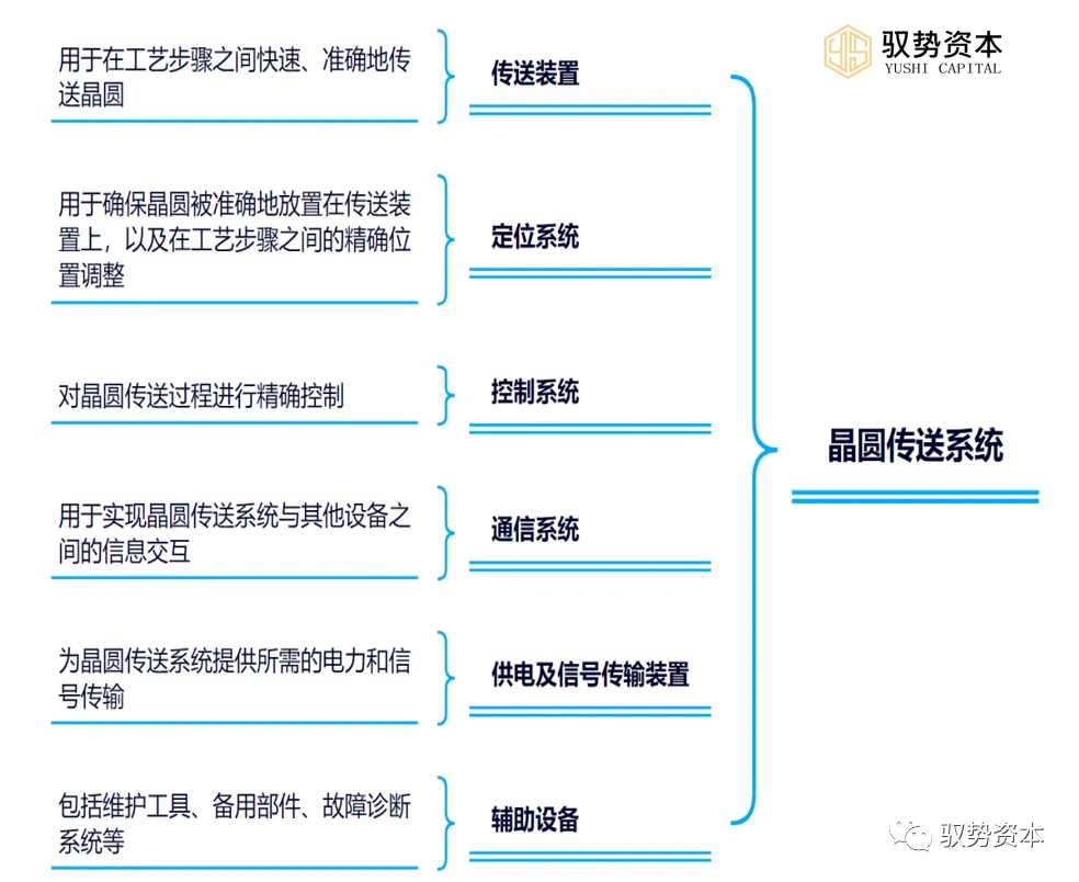
1) Transport Device: Includes robotic arms, conveyor belts, robots, etc., used for the rapid and accurate transport of wafers between process steps. These devices need to have high precision, high speed, and high reliability.2) Positioning System: Ensures that wafers are accurately placed on transport devices and makes precise positional adjustments between process steps. Positioning systems typically use laser ranging, image recognition, and other technologies.3) Control System: Precisely controls the wafer transport process, including path planning, speed control, collision prevention, etc. Control systems typically consist of controllers, sensors, and actuators.4) Communication System: Used to achieve information exchange between the wafer transport system and other devices, such as position information, status information, etc. Communication systems typically use wired or wireless communication technologies.5) Power Supply and Signal Transmission Devices: Provide the necessary power and signal transmission for the wafer transport system, including cables, power supplies, connecting lines, etc.6) Auxiliary Equipment: Includes maintenance tools, spare parts, fault diagnosis systems, etc., to support the normal operation and maintenance of the wafer transport system.
(8) Other Integrated Systems: Other integrated systems in semiconductor equipment mainly include cooling systems, control systems, material management systems, and software systems.
2. Midstream of the Semiconductor Industry Chain
2.1 Semiconductor Design
1. Design Content
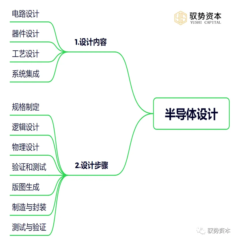
Semiconductor design involves multiple aspects, including circuit design, device design, process design, and system integration. Below, we will elaborate on these aspects in detail. (1) Circuit Design: Semiconductor circuit design is the core of semiconductor design, which involves the analysis, simulation, and optimization of electronic circuits. Designers need to use hardware description languages (such as Verilog, VHDL, etc.) to describe the circuit, and then use electronic design automation tools for logic synthesis to convert the circuit into a logic circuit diagram. During this process, designers need to continuously check and modify the program functions to ensure they meet the expected functionality.
(2) Device Design: Semiconductor device design mainly focuses on the design and optimization of semiconductor components (such as active components like diodes and passive components like resistors). This involves a deep understanding of semiconductor materials, such as the impact of resistivity and dopants. By changing the temperature and doping concentration during the manufacturing process, the conductivity of semiconductors can be easily altered, optimizing device performance.
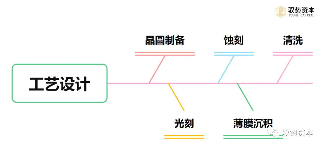
(3) Process Design: Semiconductor process design involves the entire manufacturing process of semiconductors, including wafer preparation, photolithography, etching, thin film deposition, cleaning, and other steps. Each step requires precise process control to ensure the performance and quality of the final product. Additionally, process design needs to consider manufacturing costs and efficiency to achieve commercial production.
(4) System Integration: System integration is the final stage of semiconductor design, integrating all designed parts into a complete system. This requires consideration of compatibility, power consumption, heat dissipation, and other issues between various parts. At the same time, system testing and verification are needed to ensure that the system’s functionality and performance meet design requirements.
Overall, semiconductor design knowledge is a comprehensive field involving knowledge from multiple disciplines, including electronic engineering, materials science, and physics. Designers need a solid theoretical foundation and rich practical experience to tackle increasingly complex semiconductor design challenges.
2. Design Steps
The steps of semiconductor design typically include the following: (1) Specification Development: First, the design requirements and specifications need to be clarified, including performance indicators, power consumption, costs, and other requirements.
(2) Logic Design: Based on specification requirements, logic design and hardware description language (HDL) writing are performed. Common HDLs include Verilog and VHDL. By writing HDL, the circuit functionality is described, and logical functionality verification and simulation testing are conducted.
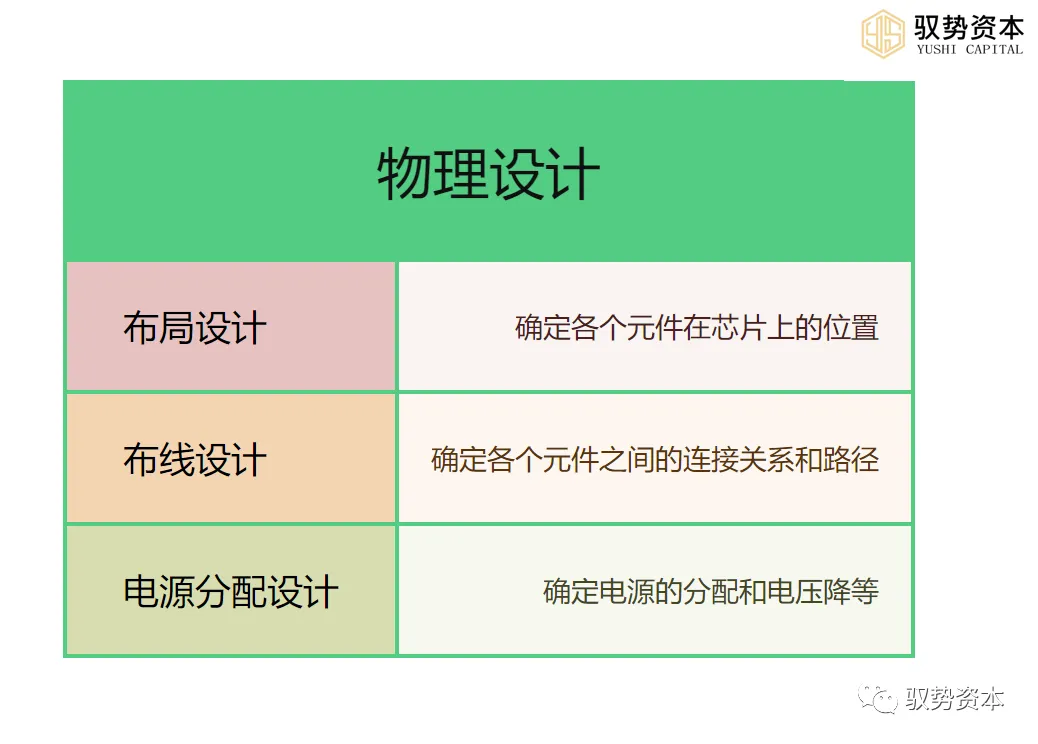
(3) Physical Design: Based on logic design, physical design is performed. This includes layout design, routing design, and power distribution design. Layout design determines the positions of various components on the chip, routing design determines the connections and paths between components, and power distribution design determines the distribution of power and voltage drops.
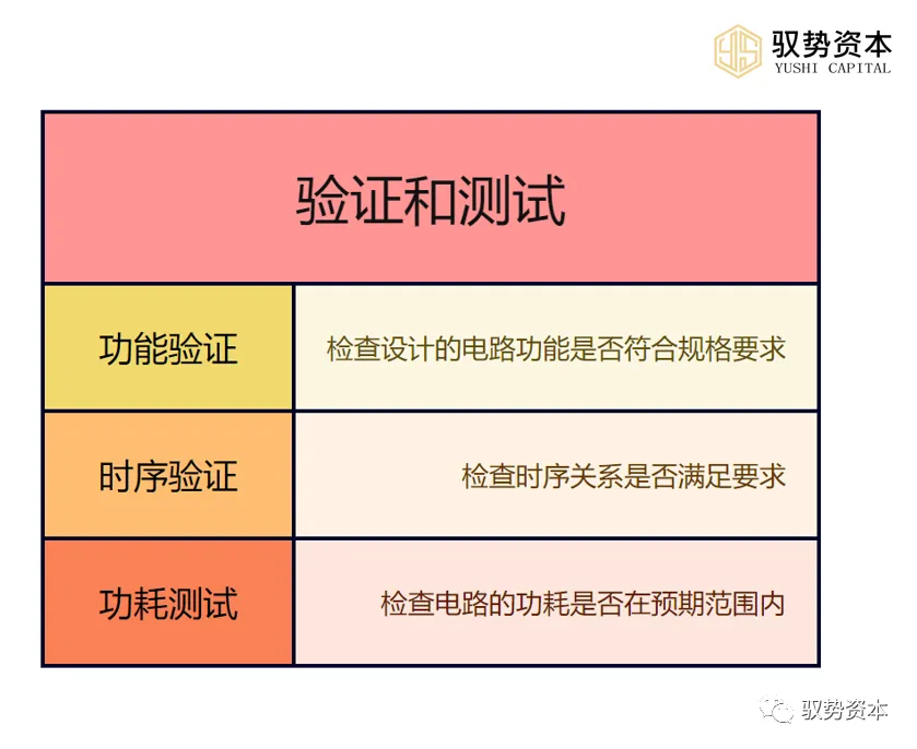
(4) Verification and Testing: After completing the physical design, verification and testing are needed. This includes functional verification, timing verification, power consumption testing, etc. Functional verification checks whether the designed circuit functions meet specification requirements, timing verification checks whether timing relationships meet requirements, and power consumption testing checks whether the circuit’s power consumption is within the expected range.
(5) Layout Generation: After verification and testing, the design results are converted into layouts, including circuit diagrams, layout diagrams, routing diagrams, etc. Layout generation is one of the important steps in semiconductor manufacturing, requiring consideration of manufacturing processes and costs.
(6) Manufacturing and Packaging: The generated layouts are sent to manufacturing plants for production and packaging. The manufacturing process includes multiple steps, such as thin film deposition, photolithography, etching, doping, etc. Packaging involves encapsulating and protecting the manufactured chips to enable communication and control with the outside world.
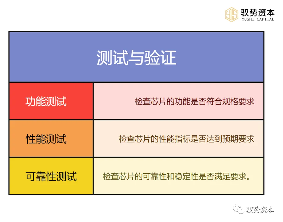
(7) Testing and Verification: After manufacturing and packaging are completed, testing and verification are needed. This includes functional testing, performance testing, reliability testing, etc. Functional testing checks whether the chip’s functionality meets specification requirements, performance testing checks whether the chip’s performance indicators meet expected requirements, and reliability testing checks whether the chip’s reliability and stability meet requirements.
Overall, the steps of semiconductor design are a complex and detailed process that requires multiple stages of verification and testing to ensure the correctness and reliability of the design. Meanwhile, with the continuous development of technology, the steps of semiconductor design are also continuously improving and perfecting.
2.2 Semiconductor Manufacturing
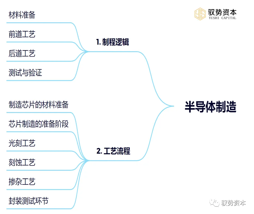
1. Process Logic
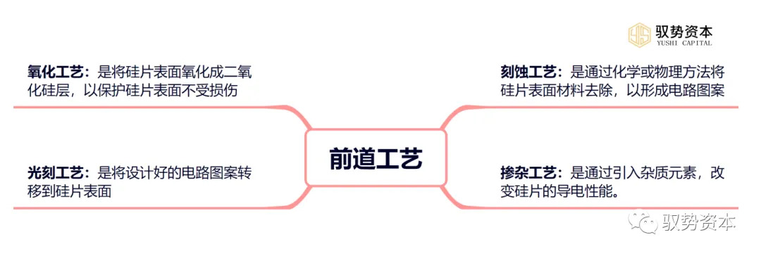
The process logic of semiconductor manufacturing can be summarized in the following points: (1) Material Preparation: To manufacture semiconductor devices, the corresponding materials must first be prepared. Generally, semiconductor materials are high-purity single-crystal silicon, used as the base material for manufacturing integrated circuits, transistors, solar cells, and other semiconductor devices. To obtain high-purity single-crystal silicon, special methods like the Czochralski method or floating-zone melting method are used for preparation. (2) Front-end Processes: In the manufacturing of semiconductor devices, front-end processes are one of the key links. They include oxidation, photolithography, etching, doping, and other steps. The oxidation process oxidizes the surface of the silicon wafer into a silicon dioxide layer to protect the surface from damage; the photolithography process transfers the designed circuit pattern onto the surface of the silicon wafer; the etching process removes surface materials not protected by the photoresist through chemical or physical methods to form the circuit pattern; the doping process introduces impurity elements to change the conductivity of the silicon wafer.
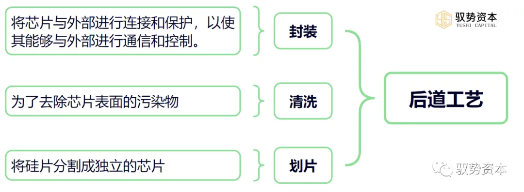
(3) Back-end Processes: The back-end processes are another key link in manufacturing semiconductor devices. They include dicing, cleaning, and packaging steps. Dicing involves cutting the silicon wafer into individual chips; cleaning is to remove contaminants from the chip surface; packaging connects and protects the chip to enable communication and control with the outside world.
(4) Testing and Verification: After manufacturing is complete, semiconductor devices need to undergo testing and verification. This includes functional testing, performance testing, reliability testing, etc., to ensure they meet design requirements and quality standards. Overall, the process logic of semiconductor manufacturing is to transform raw materials into semiconductor devices that meet specific specifications and requirements through a series of meticulous operations and high levels of skill and experience. Each link requires strict quality control and management to ensure product quality and performance reach the highest levels.
2. Process Flow
The process flow of semiconductor manufacturing mainly includes the following steps: (1) Preparation of Materials for Chip Manufacturing: High-purity single-crystal silicon is used as the base material for manufacturing chips. Single-crystal silicon is formed by melting silicon at high temperatures and slowly cooling it down. (2) Preparation Phase for Chip Manufacturing: Before manufacturing chips, a series of preparatory work is needed. First, single-crystal silicon needs to be cut into silicon wafers of specified sizes and polished and cleaned to remove surface impurities and defects. Next, coating and drying are needed to form a thin film on the surface of the silicon wafer, which will act as a photoresist to protect the underlying silicon wafer from corrosion and etching effects.(3) Photolithography Process: The photolithography process is one of the core links in chip manufacturing. In the photolithography process, patterns from the mask are transferred onto the silicon wafer using photoresist. The mask is a glass plate with patterns, using controlled light transmission and reflection to transfer the patterns onto the silicon wafer. The photolithography process requires precise optical systems and advanced computer technologies to achieve high-precision pattern transfers.(4) Etching Process: The etching process is another core link in chip manufacturing. In the etching process, chemical reagents or plasma are used to remove materials from the silicon wafer surface that are not protected by photoresist. By controlling the etching time and depth, precise machining and shape control of the silicon wafer can be achieved.(5) Doping Process: The doping process introduces impurities into semiconductor materials. In semiconductor manufacturing, doping is performed to change the conductivity of semiconductors. Doping processes usually use ion implantation or diffusion methods. By controlling the type and concentration of dopants, the conductivity type and capability of semiconductors can be controlled.(6) Packaging and Testing Phase: After chip manufacturing is complete, packaging and testing are needed. Packaging is the process of connecting and protecting the chip with the outside world. During the packaging process, the chip is placed in a packaging body and connected to the outside via pins or other means. Testing checks whether the chip’s functionality and performance meet design requirements.
3. Downstream of the Semiconductor Industry Chain
3.1 Medical Field
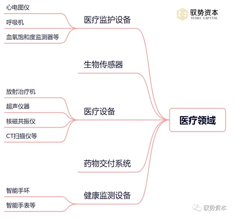
(1) Medical Equipment: Semiconductor technology is widely used in various medical devices, such as radiation therapy machines, ultrasound instruments, MRI machines, CT scanners, etc. Semiconductor devices enable these machines to detect and process images, sounds, and signals in real-time, providing more accurate and faster diagnostic results.
(2) Biosensors: Biosensors are devices that use semiconductor technology to monitor and detect chemical and biological changes in the body. These sensors can detect blood glucose levels, heart rates, blood pressures, and other physiological indicators, transmitting data to medical professionals for analysis and processing.
(3) Medical Monitoring Devices: Semiconductor technology is used to develop various monitoring devices, such as electrocardiograms, ventilators, blood oxygen saturation monitors, etc. These devices use semiconductor sensors and microprocessors to monitor patients’ physiological parameters and provide therapeutic support when necessary.
(4) Drug Delivery Systems: Semiconductor technology can be used to develop intelligent drug delivery systems that release drugs according to specified times and dosages. These systems can provide personalized treatment based on patients’ needs and improve drug absorption efficiency.
(5) Health Monitoring Devices: In recent years, semiconductor technology has been widely used in health monitoring devices, such as smart bracelets, smartwatches, etc. These devices can monitor movement, sleep quality, heart rates, and other physiological indicators, transmitting data to smartphones or the cloud for analysis and tracking.
3.2 Electronics Field
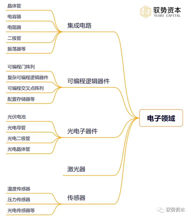
(1) Integrated Circuits (ICs): Semiconductor materials (usually silicon) are used to manufacture integrated circuits, also known as chips. Chips are the core of electronic devices, capable of containing millions of transistors, capacitors, resistors, diodes, oscillators, and other electronic components. ICs are widely used in computers, smartphones, tablets, televisions, audio devices, and other electronic products.
(2) Programmable Logic Devices (PLDs): Semiconductor devices such as programmable gate arrays, complex programmable logic devices, programmable crosspoint arrays, configuration memory, etc., are used to implement digital logic circuits, such as logic gates, sequential circuits, etc. PLDs are widely used in both analog and digital systems.3) Optoelectronic Devices: Semiconductor materials can convert light energy into electrical energy or vice versa. Optoelectronic devices such as photovoltaic cells (solar cells), photoconductive tubes, photodiodes, and phototransistors are widely used in solar power generation, optical communication, and optoelectronic displays.
(4) Lasers: Lasers are devices made from semiconductor materials that can emit amplified and focused laser beams. Lasers are widely used in medical, communication, and material processing fields, such as laser cutting, laser printing, and laser medical treatment.
(5) Sensors: Semiconductor sensors can convert physical signals (such as temperature, pressure, light, etc.) into electrical signals for measurement and detection. Common semiconductor sensors include temperature sensors, pressure sensors, photonic sensors, etc., widely used in automotive, medical, and environmental monitoring fields.
3.3 Communication Field
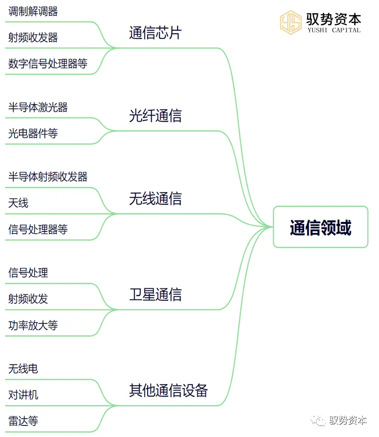
(1) Communication Chips: Semiconductor technology plays a central role in communication chips. Communication chips include modems, RF transceivers, digital signal processors, etc., used to implement wireless and wired communication functionalities. These chips are widely used in mobile phones, routers, modems, and other communication devices.
(2) Fiber Optic Communication: Fiber optic communication is a technology that transmits data using light signals. Semiconductor lasers and photonic devices are used to send and receive light signals. Fiber optic communication has advantages such as high capacity, long-distance transmission, and low loss, widely used in telephone networks, the internet, and television signal transmission.
(3) Wireless Communication: Wireless communication includes technologies such as Bluetooth, Wi-Fi, mobile communications, etc., in which semiconductor devices play important roles. Semiconductor RF transceivers, antennas, signal processors, etc., are used in wireless communication devices, playing significant roles in achieving wireless data transmission and high-speed communication.
(4) Satellite Communication: Satellite communication is a communication method that uses artificial satellites for data transmission, in which semiconductor technology plays a key role. Semiconductor devices are used for signal processing, RF transmission, power amplification, etc., enabling high-speed data transmission and communication connections between satellites and the ground.
(5) Other Communication Devices: Semiconductor technology is also applied in other communication devices, such as radios, walkie-talkies, and radar systems. Semiconductor devices are used to implement signal transmission, amplification, processing, and demodulation functions, improving the performance and reliability of communication devices.
3.4 Internet of Things (IoT) Field
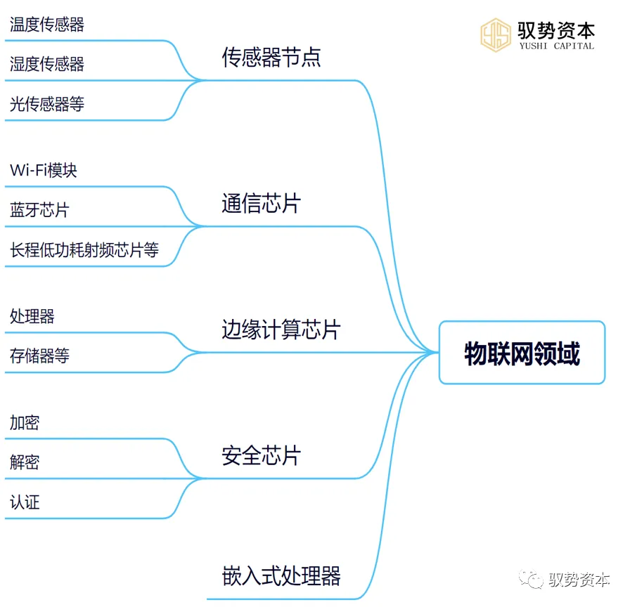
(1) Sensor Nodes: The key components of the Internet of Things are sensors used to perceive and collect various data from the environment. Semiconductor sensors are widely used in IoT devices, such as temperature sensors, humidity sensors, light sensors, etc. These sensors convert physical signals into electrical signals through semiconductor devices and transmit data to other devices for processing and decision-making.
(2) Communication Chips: IoT devices need to implement data transmission and connectivity, and semiconductor communication chips play a crucial role. Communication chips, such as Wi-Fi modules, Bluetooth chips, long-range low-power RF chips, etc., enable IoT devices to communicate, interact, and connect with the internet and other devices.
(3) Edge Computing Chips: A large amount of data in the IoT needs to be processed and computed locally on devices to reduce data transmission delays and lower cloud computing burdens. Edge computing chips integrate processors, memory, and other functions, enabling local data analysis and decision-making on IoT devices, providing real-time feedback and intelligent control.
(4) Security Chips: IoT devices face security issues such as network attacks and data breaches, and to protect device and user data security, semiconductor security chips are widely applied. Security chips have encryption, decryption, and authentication functions, ensuring secure communication between devices and the cloud, preventing unauthorized access and attacks.
(5) Embedded Processors: IoT devices need to perform data processing, control, and decision-making, and semiconductor embedded processors provide efficient computing and control capabilities. Embedded processors, such as ARM chips, are widely used in IoT devices, offering low power consumption and sufficient computing performance.
3.5 Automotive Field
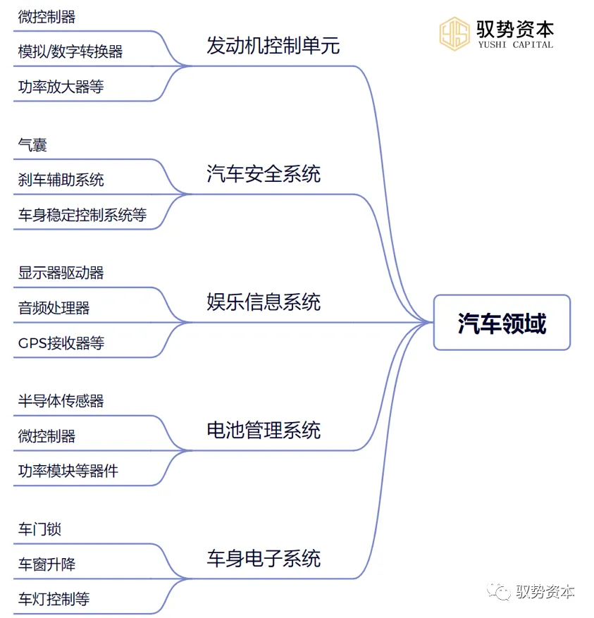
(1) Engine Control Unit (ECU): The engine control unit is the core part of automotive electronic systems, responsible for controlling the fuel supply, ignition timing, emission control, and other functions of the engine. The ECU integrates many semiconductor devices, such as microcontrollers, analog/digital converters, power amplifiers, etc., to achieve precise control over the engine.
(2) Automotive Safety Systems: Automotive safety systems, such as airbags, brake assist systems, body stability control systems, etc., require semiconductor devices. These systems use semiconductor sensors, microcontrollers, power modules, etc., to monitor and control the vehicle’s operating status, enhancing vehicle safety performance.
(3) Entertainment Information Systems: Modern vehicles are generally equipped with entertainment information systems, including navigation, audio, rearview cameras, and other functions. These systems require semiconductor devices, such as display drivers, audio processors, GPS receivers, etc.
(4) Battery Management Systems: New energy vehicles, such as electric vehicles, require battery management systems to monitor and manage battery charge and discharge status, temperature, voltage, and other parameters. Battery management systems require semiconductor sensors, microcontrollers, power modules, and other devices.
(5) Body Electronic Systems: Automotive body electronic systems include functions such as door locks, window lifts, and light control. These systems require semiconductor devices, such as microcontrollers, power amplifiers, sensors, etc.
3.6 New Energy Field
(1) Solar Cells: Semiconductor materials are the core components for manufacturing solar cells, especially silicon materials, which are widely used to manufacture high-efficiency solar cells. By converting solar energy into electrical energy, semiconductor materials enable solar cells to provide clean and renewable energy for people’s lives and industrial production. (2) Wind Energy Control: In wind power generation systems, semiconductor materials also play an important role. For example, semiconductor power modules can be used to control the operation of generators, improving generator efficiency and enhancing system reliability. (3) New Energy Vehicles: In new energy vehicles, semiconductor materials are widely applied in battery management systems, motor control systems, and charging systems. For example, semiconductor sensors can be used to monitor battery status, ensuring safe operation of the battery. (4) Energy Storage Systems: Semiconductors can be used to improve the efficiency and reliability of energy storage systems. For instance, power modules can be used to enhance charging and discharging efficiency of batteries. Additionally, semiconductor materials can be utilized in various electronic components used in battery management systems and charging systems. (5) Power Devices: In the new energy field, the application of semiconductor power devices is becoming increasingly widespread. For example, in photovoltaic power plants, power devices are used to enhance the output power of photovoltaic cells and reduce losses; in wind power generation, power devices are used to improve wind energy utilization and generator efficiency. Furthermore, power devices are widely used in new energy vehicles, energy storage systems, and other fields.
▌Produced by Xiamen Torch High-tech Zone News Promotion Center
▌Source: Yushi Capital
▌Editor: Li Shun
▌Reviewed by: Guan Xuan
▌Reprint with acknowledgment丨Xiamen Torch High-tech Zone