1
Concept of Advanced Semiconductor Packaging Industry
(1) Concept
Packaging is the final process in semiconductor manufacturing. Semiconductor packaging is the process of further processing tested wafers to obtain independent chips, with the aim of adding functionality to the chip’s contacts that can connect to external circuits, such as adding pins to connect with external circuits like PCB boards. Meanwhile, packaging can provide a “protective shell” for the chip, preventing physical or chemical damage. The testing phase after packaging confirms the electrical functionality of the chips. Packaging can be divided into traditional packaging and advanced packaging. Advanced packaging is a process where wafers are packaged and then cut. Compared to traditional packaging, advanced packaging has advantages such as miniaturization, lightweight, high density, low power consumption, and functional integration, which can not only enhance performance, expand functionality, and optimize form but also reduce costs compared to system-level chips.
(2) Position in the Industry Chain
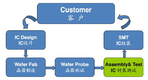
The semiconductor manufacturing process includes chip design, wafer manufacturing, and packaging testing. In the industry chain, packaging is located downstream of wafer manufacturing and upstream of module manufacturing. Packaging can be considered the last process in semiconductor production, laying out, bonding, and fixing the chip (Die) on different types of frames or substrates, leading out the terminals and fixing them into different shaped packages using encapsulation materials (EMC).
2
Advanced Semiconductor Packaging Industry
Market Status Analysis
(1) Global Advanced Semiconductor Packaging Market Size
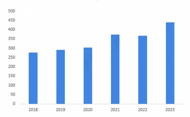
Advanced packaging has advantages such as miniaturization, lightweight, high density, low power consumption, and functional integration. In the current development environment of the chip industry, it can enhance chip performance to a higher level at a lower cost, showing great potential for development, with a steadily growing market size. According to data disclosed by Yole, the global advanced packaging market share in 2023 is $43.9 billion, a year-on-year increase of 19.62%, with a rapid growth rate.
(2) Global Advanced Semiconductor Packaging Industry Development Trends
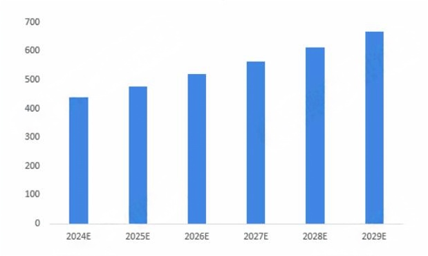
As the downstream markets of advanced packaging, such as integrated circuits and optoelectronic devices, are expected to recover, the demand for the global advanced packaging market will further expand. According to relevant institutions, it is expected that the global advanced packaging industry market size will reach $66 billion by 2029, with a compound annual growth rate (CAGR) of 8.7%.
3
China’s Advanced Semiconductor Packaging Industry
Competitive Landscape
(1) Competitive Tier of China’s Advanced Semiconductor Packaging Industry
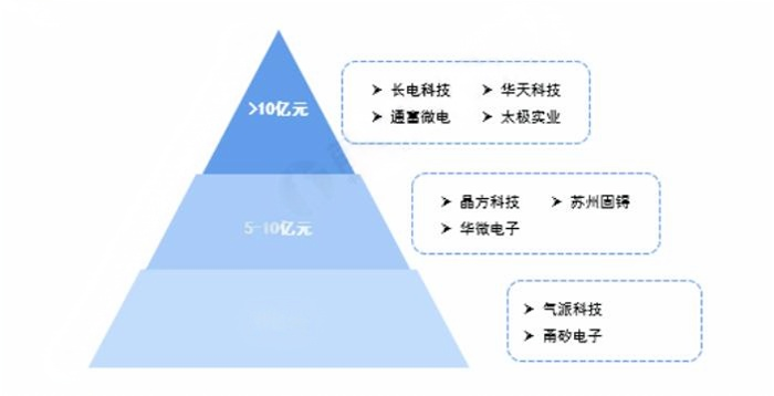
Advanced packaging can be divided into three competitive tiers based on registered capital scale. Among them, companies with registered capital greater than 1 billion yuan include Changjiang Electronics Technology, Tongfu Microelectronics, Huatian Technology, and Taiji Industry; companies with registered capital between 500 million and 1 billion yuan include Jingfang Technology, Huayi Electronics, and Suzhou Goodix; and the remaining companies have registered capital below 500 million yuan.
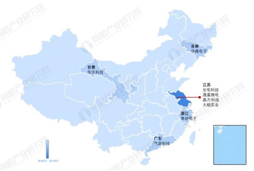
(2) Distribution of Leading Enterprises in China’s Advanced Semiconductor Packaging Industry
According to the distribution of leading enterprises in advanced packaging, Jiangsu Province has the most listed companies in the industry, including Changjiang Electronics Technology and Tongfu Microelectronics, which are the two most representative advanced packaging companies in China. The remaining listed companies are located in Gansu, Jilin, Zhejiang, and Guangdong.