The third-generation semiconductors, also known as wide bandgap semiconductors, are represented by silicon carbide (SiC) and gallium nitride (GaN). They possess superior properties such as high frequency, high efficiency, high power, high voltage resistance, high temperature resistance, and strong radiation resistance. These characteristics align with national strategic needs for energy conservation, intelligent manufacturing, and information security. They are key core materials and electronic components supporting the independent innovation and transformation of industries such as the new generation of mobile communications, new energy vehicles, high-speed rail trains, and energy internet, becoming the focal point of global semiconductor technology and industry competition.
[1]
Three Generations of Semiconductor Materials from the Perspective of Energy Bands
The third-generation semiconductor materials exhibit significantly better performance than the first-generation (silicon (Si), germanium (Ge)) and second-generation (gallium arsenide (GaAs)) semiconductor materials in the fields of high power, high temperature, high frequency, and radiation resistance in microelectronics, as well as in short-wavelength optoelectronic fields. Third-generation semiconductor materials are becoming a strategic high ground for seizing the next generation of information technology, energy-saving technologies, and national defense security technologies, and are an important component of strategic emerging industries.
From the perspective of energy bands, semiconductor materials can also be divided into three generations.
The first-generation semiconductor materials are represented by elemental semiconductors such as silicon and germanium. Their typical application is integrated circuits, primarily used in low-voltage, low-frequency, low-power transistors and detectors. For the foreseeable future, silicon semiconductor materials will still maintain their dominant position. However, the physical properties of silicon limit its applications in optoelectronics and high-frequency electronic devices, as its indirect bandgap characteristic prevents it from achieving high electro-optical conversion efficiency. Additionally, its narrow bandgap width (1.12 eV) and low saturation electron mobility (1450 cm²/V·s) hinder the development of high-frequency and high-power electronic devices.
The second-generation semiconductor materials are represented by gallium arsenide and indium phosphide (InP). The electron mobility of gallium arsenide is six times that of silicon, and it has a direct bandgap, making its devices exhibit high-frequency and high-speed optoelectronic performance compared to silicon devices, which is recognized as a suitable communication semiconductor material. Meanwhile, its application in military electronic systems is increasingly widespread and irreplaceable. However, its bandgap width only covers 1.35 eV (InP) to 2.45 eV (AlP), which can only cover red light wavelengths from 506 to 918 nm and longer wavelengths, failing to meet the needs of mid and short-wavelength optoelectronic devices. Due to the insufficient bandgap width of second-generation semiconductor materials and their low breakdown electric field, their application in high-temperature, high-frequency, and high-power devices is severely limited. Furthermore, the toxicity of GaAs materials may pose environmental pollution issues and potential threats to human health.
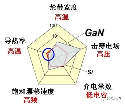
The third-generation semiconductor materials refer to III-nitride materials (such as gallium nitride (GaN), aluminum nitride (AlN), etc.), silicon carbide, oxide semiconductors (such as zinc oxide (ZnO), gallium oxide (Ga₂O₃), perovskite (CaTiO₃), etc.), and diamond, which are all wide bandgap semiconductor materials. Compared to the first and second generations, third-generation semiconductor materials have a large bandgap width, high breakdown electric field, high thermal conductivity, high electron saturation velocity, and strong radiation resistance. Therefore, semiconductor devices made from third-generation semiconductor materials can not only operate stably at higher temperatures but are also more reliable under high voltage and high frequency conditions. Additionally, they can achieve higher operational capabilities with less energy consumption.
[2]
Development Potential of Gallium Nitride (GaN) Materials
Gallium nitride is a wide bandgap material that can provide performance advantages similar to silicon carbide (SiC) but with greater potential for cost reduction. The industry believes that in the coming years, the cost of GaN power devices is expected to decrease to the same price level as silicon MOSFETs, IGBTs, and rectifiers.
GaN power electronic devices have advantages such as higher operating voltage, higher switching frequency, and lower conduction resistance, and can be integrated with silicon-based semiconductor integrated circuit processes that are extremely low in cost and highly mature. They have enormous development potential in the new generation of high-efficiency, compact power conversion and management systems, electric locomotives, industrial motors, and other fields.
Due to the growing demand for high-speed, high-temperature, and high-power semiconductor devices, the semiconductor industry is re-evaluating the designs and materials used in semiconductors. With the continuous emergence of various faster and smaller computing devices, silicon materials have struggled to maintain Moore’s Law. The unique advantages of gallium nitride materials, such as excellent noise figures, high maximum currents, high breakdown voltages, and high oscillation frequencies, provide unique options for various applications in military, aerospace, defense, automotive fields, as well as in high-power fields like industrial, solar power, and wind energy.
As gallium nitride optoelectronic semiconductors are used in military, aerospace, defense, and consumer electronics, optoelectronic semiconductors have become the main product type in the global gallium nitride semiconductor device market, occupying an absolute dominant position. Among them, power semiconductor devices are expected to become the fastest-growing devices in the future due to the increasing industrial demand for high-power devices.
For the development of GaN power devices, market demand traction is crucial. From the power supply and PFC (Power Factor Correction) fields that will dominate the market in 2020 to UPS (Uninterruptible Power Supply) and motor drives, many application areas will benefit from the characteristics of GaN-on-Si power devices.
Market research firm Yole Développement believes that in addition to these applications, pure electric vehicles (EVs) and hybrid electric vehicles (HEVs) will also begin to adopt these new materials and devices after 2020. In terms of market size, the overall market for GaN devices could reach approximately $600 million by 2020. At that time, a 6-inch wafer could process about 580,000 GaN devices. Given the expectation that EVs and HEVs will start adopting GaN from 2018 or 2019, the number of GaN devices is expected to increase significantly from 2016, with an annual growth rate (CAGR) of 80% until 2020.
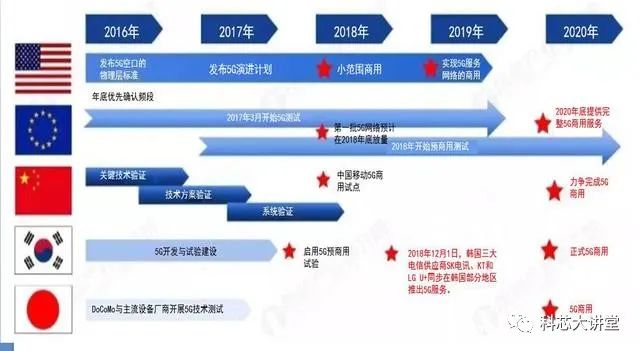
As 5G technology matures, it brings business opportunities to the RF Front End chip market. The demand for RF power amplifiers (RF PA) will continue to grow, where traditional laterally diffused metal oxide semiconductor (LDMOS) processes will gradually be replaced by gallium nitride (GaN), especially under 5G technology which requires support for more components and higher frequencies, while gallium arsenide (GaAs) will grow relatively steadily. Through the introduction of new RF technologies, RF PA will achieve new process technologies, where GaN RF PA will become the mainstream process technology for output power above 3W, while LDMOS market share will gradually decline.
Because 5G technology encompasses millimeter-wave frequencies and large-scale MIMO (Multi-Input Multi-Output) antenna applications to achieve breakthroughs in 5G wireless integration and architecture, how to massively adopt Massive-MIMO and millimeter-wave backhaul systems will be key to development. Due to the high frequency of 5G, the demand for high-power, high-performance, and high-density RF components is increasing, among which gallium nitride (GaN) meets these conditions, thus the GaN market presents greater potential business opportunities.
[3]
What is Gallium Nitride (GaN)?
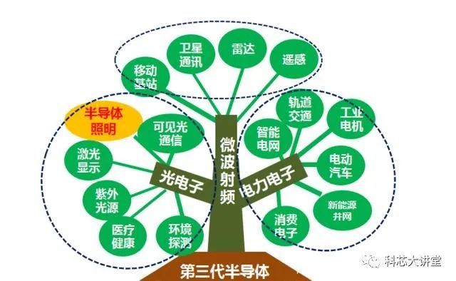
The research and application of GaN materials are currently at the forefront and hotspot of global semiconductor research, being a new type of semiconductor material for developing microelectronic devices and optoelectronic devices. Together with SiC and diamond, it is known as the third generation of semiconductor materials following the first generation of Ge and Si semiconductor materials and the second generation of GaAs and InP compound semiconductor materials. It has properties such as a wide direct bandgap, strong atomic bonds, high thermal conductivity, good chemical stability (almost not corroded by any acid), and strong radiation resistance, making it have broad prospects in applications involving optoelectronics, high-temperature high-power devices, and high-frequency microwave devices.
Gallium nitride (GaN) is a typical representative of third-generation semiconductor materials, serving as a core component in semiconductor lighting, particularly in light-emitting diodes (LEDs) at T=300K. Gallium nitride is a synthetic material, and the conditions for its natural formation are extremely harsh, requiring temperatures over 2000 degrees Celsius and pressures near ten thousand atmospheres to synthesize GaN from metallic gallium and nitrogen, which is impossible to achieve in nature.
As we all know, the first generation of semiconductor materials is silicon, which mainly addresses data computation and storage issues; the second generation of semiconductors is represented by gallium arsenide, which is applied in fiber optic communications, mainly addressing data transmission issues; while the third generation of semiconductors is represented by gallium nitride, which excels in the conversion of electricity and light and has higher efficiency in microwave signal transmission, thus can be widely applied in lighting, displays, communications, and other major fields. In 1998, American scientists developed the first gallium nitride transistor.
[4]
Performance Characteristics of Gallium Nitride (GaN)
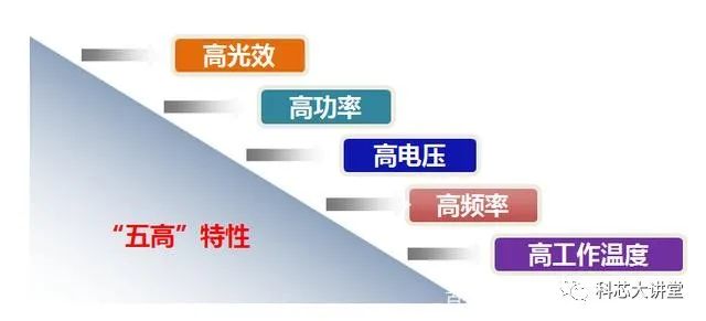
High performance: This mainly includes high output power, high power density, high operating bandwidth, high efficiency, small size, and light weight. Currently, the first and second generation semiconductor materials have reached their limits in output power, while GaN semiconductors, due to their advantages in thermal stability, can easily achieve high operating pulse widths and high duty cycles, increasing the radiated power of antenna units by ten times.
High reliability: The lifespan of power devices is closely related to their temperature; the higher the junction temperature, the shorter the lifespan. GaN materials have high junction temperatures and high thermal conductivity, greatly improving the adaptability and reliability of devices at different temperatures. GaN devices can be used in military equipment above 650°C.
Low cost: The application of GaN semiconductors can effectively improve the design of transmitting antennas, reduce the number of transmitting components and amplifier stages, and effectively lower costs. Currently, GaN has begun to replace GaAs as the electronic device material for new radar and jamming machine T/R (transmit/receive) modules. The next generation of AMDR (Active Electronically Scanned Array Radar) by the U.S. military will utilize GaN semiconductors. Gallium nitride has wide bandgap, high breakdown voltage, high thermal conductivity, high electron saturation drift velocity, strong radiation resistance, and good chemical stability, making it theoretically the highest efficiency material system for electro-optical and optoelectronic conversion, and a key foundational material for manufacturing wide spectrum, high power, and high efficiency microelectronic, power electronic, and optoelectronic devices.
GaN’s wide bandgap (3.4 eV) and substrates like sapphire lead to good heat dissipation performance, facilitating the operation of devices under high power conditions. With ongoing research and development of III-nitride materials and devices, GaInN ultra-bright blue and green LED technology has already been commercialized, and now major companies and research institutions around the world are investing heavily to join the competition in developing blue LEDs.
[5]
Applications of Gallium Nitride
1. New Electronic Devices
The GaN material series has low thermal generation rates and high breakdown fields, making it an important material for developing high-temperature high-power electronic devices and high-frequency microwave devices. Currently, with advancements in MBE technology in GaN material applications and breakthroughs in key thin film growth technologies, various heterostructures of GaN have been successfully grown. New devices such as metal-semiconductor field-effect transistors (MESFETs), heterojunction field-effect transistors (HFETs), and modulation-doped field-effect transistors (MODFETs) have been developed using GaN materials. The modulation-doped AlGaN/GaN structure has high electron mobility (2000 cm²/V·s), high saturation velocity (1×10⁷ cm/s), and relatively low dielectric constant, making it a preferred material for microwave devices; GaN’s wide bandgap (3.4 eV) and substrates like sapphire lead to good heat dissipation performance, facilitating the operation of devices under high power conditions.
2. Optoelectronic Devices
The GaN material series is an ideal material for short-wavelength light-emitting devices, with the bandgap of GaN and its alloys covering the spectral range from red to ultraviolet light. Since the development of the first homojunction GaN blue LED in Japan in 1991, ultra-bright blue LEDs with InGaN/AlGaN double heterojunctions and InGaN single quantum well GaN LEDs have been successively developed. Currently, Zcd and 6cd single quantum well GaN blue and green LEDs have entered mass production, filling the long-standing market gap for blue LEDs.
Blue light-emitting devices have a huge application market in high-density optical disc information storage, all-optical displays, laser printers, and more. As research and development work on III-nitride materials and devices continues to deepen, GaInN ultra-bright blue and green LED technology has been commercialized, with major companies and research institutions around the world investing heavily to join the competition in developing blue LEDs.
In 1993, Nichia Corporation first developed high-brightness GaInN/AlGaN heterojunction blue LEDs with brightness exceeding LCDs, using Zn-doped GaInN as the active layer, achieving an external quantum efficiency of 2.7%, with a peak wavelength of 450 nm, and commercializing the product. In 1995, the company launched a GaN green LED product with a light output power of 2.0 mW and brightness of 6 cd, with a peak wavelength of 525 nm and a half-peak width of 40 nm. Recently, the company has also introduced white solid-state lighting devices with a color temperature of 6500K and an efficiency of 7.5 lumens/W using its blue LED and phosphor technologies. In addition to Nichia, companies like HP and Cree have also launched their high-brightness blue LED products. The high-brightness LED market is expected to grow from $386 million in 1998 to $1 billion in 2003. The applications of high-brightness LEDs mainly include automotive lighting, traffic signals, outdoor road signs, flat-panel displays, high-density DVD storage, and blue-green light for underwater communication.
After successfully developing III-nitride blue LEDs, research has shifted focus to the development of III-nitride blue LED devices. Blue LEDs have broad application prospects in optical sensing and high-density optical storage of information. Currently, Nichia Corporation holds a leading position in the GaN blue LED market, with its GaN blue LEDs achieving continuous operation at 2 mW at room temperature with a lifespan exceeding 10,000 hours. HP has successfully developed GaInN blue LEDs using sapphire substrates with optical ridge waveguide refractive index guiding. Cree Research was the first to report a CWRT blue laser on SiC, featuring a lateral device structure. Following Nichia, Cree Research, and Sony, Fujitsu announced the development of InGaN blue lasers capable of CW applications at room temperature, with a structure grown on SiC substrates and employing a vertical conduction structure (with P-type and N-type contacts made on the top and back surfaces of the wafer, respectively), marking the first reported vertical device structure for a CW blue laser.
In terms of detectors, GaN ultraviolet detectors have been developed with a wavelength of 369 nm, whose response speed is comparable to that of Si detectors. However, research in this area is still in its infancy. GaN detectors will have important applications in flame detection, missile warning, and more.
[6]
New Infrastructure Accelerating Gallium Nitride Development
GaN wide bandgap power electronic devices represent the development direction of the power electronic device field, with many material and process issues still to be resolved. Even if these issues are resolved, their prices will still be higher than those of silicon-based devices. It is expected that by 2019, the price of silicon-based GaN may fall to levels comparable to those of silicon materials. Due to their superior characteristics, they may mainly be used in mid-to-high-end applications, and just as silicon fully controlled devices will not completely replace silicon semi-controlled devices, SiC and GaN wide bandgap power electronic devices are also unlikely to fully replace silicon power MOSFETs, IGBTs, and GTOs (including IGCTs) in the future. SiC power electronic devices will mainly be used in high-voltage industrial applications above 1200V; GaN power electronic devices will mainly be used in consumer electronics and computer/server power applications below 900V.
As a third-generation semiconductor material, GaN’s properties determine that it will be more suitable for applications in technologies like 5G. From the current market situation, GaAs is still the mainstream for mobile terminal PAs and LNAs, while LDMOS dominates RF in base stations. However, as the performance of silicon materials and GaAs materials gradually reaches their limits, we expect GaN semiconductors to be increasingly applied in the wireless communication field.
Third-generation semiconductor RF electronic devices have achieved large-scale applications in both civilian and military fields. In particular, due to their advantages in high frequency, high power, and large bandwidth, gallium nitride RF electronic devices and modules play an irreplaceable role in the construction of 5G mobile communication base stations. The acceleration of 5G construction in our country will trigger rapid growth in the demand for gallium nitride RF electronic devices.
▌Produced by Xiamen Torch High-tech Zone News Propaganda Center
▌Source: Kexin Lecture Hall
▌Editor: Li Shun
▌Review: Guan Xuan
▌Reprint must indicate丨Xiamen Torch High-tech Zone