Source: Tom Talks Chip Manufacturing
Original Author: Tom
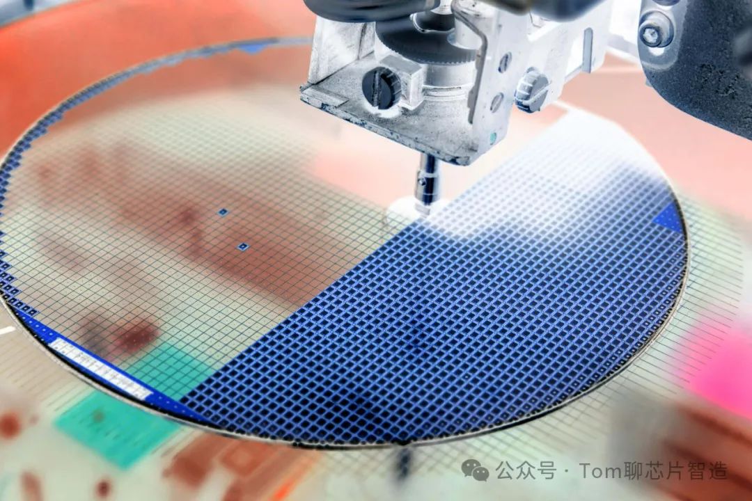
The semiconductor manufacturing process refers to the process of using semiconductor materials to manufacture chips. This process includes steps such as wafer preparation, cleaning, deposition, photolithography, etching, diffusion, annealing, electroplating, and cutting.
Semiconductor manufacturing is the process of processing wafers into complete chips that can achieve specific functions through a series of complex steps. Different chip products involve different processes, so we will systematically introduce all the semiconductor processes that may be involved in semiconductor manufacturing.
What is the boundary between semiconductor manufacturing and packaging?
The purposes of semiconductor manufacturing and packaging are different. The goal of semiconductor manufacturing (Front-end) is to produce bare wafers with complex circuit patterns, which must be done in a highly controlled cleanroom environment to prevent dust from affecting the tiny circuit structures. In contrast, the goal of packaging (Back-End of Line) is to protect the bare chips and enhance the physical strength and environmental resistance of the chips. Generally, wafer thinning is used as the boundary between manufacturing and packaging, with the thinned wafers shipped from wafer fabs to packaging factories, marking the end of the semiconductor manufacturing process.
What are the process differences among different chip products?
Chips are a broad concept and can be subdivided into many categories. They can generally be divided into logic chips (CPU, GPU, etc.), memory chips (DRAM, NAND, Flash, etc.), analog and mixed-signal chips, power devices, RF chips, sensor chips, etc.
Different types of chip products adopt different design principles, process standards, and material selections based on their application and functional requirements. For example, the advanced chip processes of 5nm and 7nm are usually used in logic chips, while in the RF chip field, SAW and BAW are not considered based on linewidth. Additionally, memory chips primarily use 12-inch wafers, but due to the limitations of SiC substrates, third-generation semiconductors commonly use 4 and 6-inch wafers.
What classifications are there for semiconductor manufacturing processes?
Includes processes such as coating, exposure, development, and baking.
Deposition: Includes PVD (Physical Vapor Deposition), CVD (Chemical Vapor Deposition), ALD (Atomic Layer Deposition). PVD includes evaporation, sputtering, and pulsed laser deposition, while CVD includes plasma-enhanced CVD (PECVD), low-pressure CVD (LPCVD), metal-organic CVD (MOCVD), MPCVD, Laser CVD, APCVD, HT-CVD, UHV CVD, etc.
Dry etching is divided into physical etching, chemical etching, and physical-chemical etching. Physical etching includes ion beam etching (IBE), while chemical etching includes plasma asher, and physical-chemical etching includes ICP-RIE, CCP-RIE, ECR-RIE, DRIE, etc.
Divided into liquid phase epitaxy (LPE), vapor phase epitaxy (VPE), molecular beam epitaxy (MBE), chemical beam epitaxy (CBE), etc.
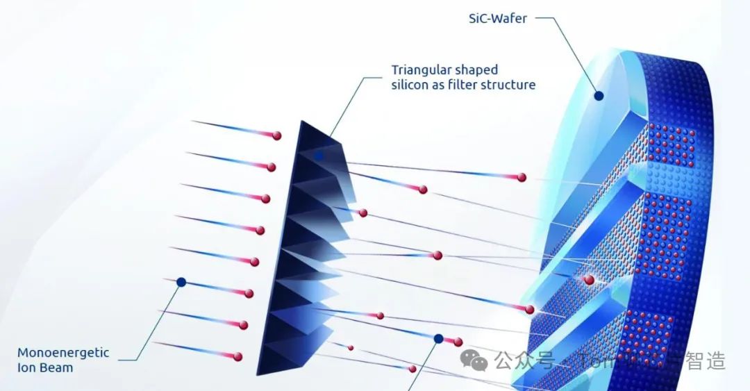
Includes high-energy ion implantation, low-energy ion implantation, high-dose ion implantation, high-throughput ion implantation, and high mass molecular ion implantation.
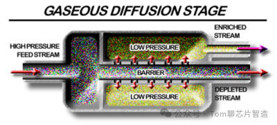
Gas source diffusion, liquid source diffusion, solid source diffusion, pre-deposition diffusion, etc.
Tube furnace annealing, rapid thermal annealing, laser annealing, plasma annealing, etc.
The wet process includes wet etching, cleaning, electroplating, chemical plating, CMP, etc.
END
The reproduced content only represents the author’s views
It does not represent the position of the Institute of Semiconductors, Chinese Academy of Sciences
Editor: Xiao Wei
Responsible Editor: Six Dollar Fish
Submission Email: [email protected]
1. The Institute of Semiconductors has made progress in the research of bionic covering neuron models and learning methods
2. The Institute of Semiconductors has made important progress in the inverted structure perovskite solar cells
3. Why is copper used as the interconnect metal in chips?
4. What exactly is the 7nm process in chips?
5. Silicon-based integrated optical quantum chip technology
6. How anomalous is the quantum anomalous Hall effect? It may lead to the next revolution in information technology!