Source: Semiconductor All Explained
Original Author: Infrared Classroom
1. What is an Integrated Circuit?
Integrated Circuit (IC) is a complex electronic system that integrates active devices such as transistors and diodes, and passive devices such as resistors and capacitors on a single semiconductor chip using a series of specific planar manufacturing processes, encapsulated in a protective shell, capable of performing specific functions.
Semiconductor planar process technology is widely used in today’s integrated circuit (IC) processes, with several main steps including:
(a) Oxidation
(b) Lithography and Etching
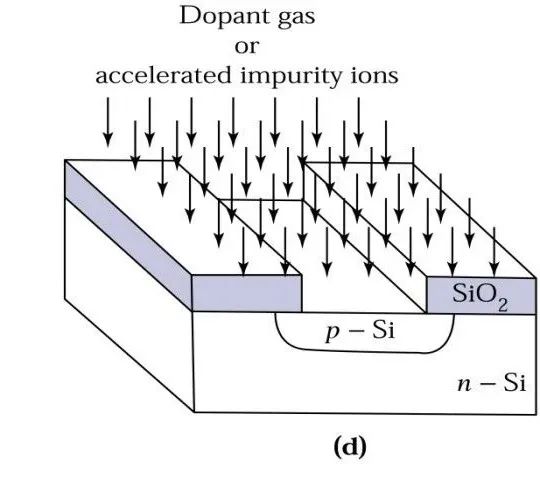
(c) Diffusion or Ion Implantation
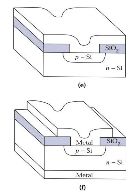
(d) Metallization.
Now let’s understand these technologies one by one:
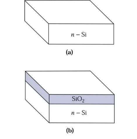
2. Oxidation
The successful development of high-quality silicon dioxide has been a major driving force in making silicon (Si) integrated circuits mainstream commercial products. Silicon dioxide can serve as an insulator for many device structures or as a barrier layer for diffusion or ion implantation during device fabrication.
For example, during the manufacturing process of a p-n junction, the silicon dioxide film can be used to define the junction area.
3. Lithography
The news about lithography machines has penetrated every aspect of semiconductors. Now, let’s understand the semiconductor lithography process.
(1) What is Lithography?
Lithography technology was first applied in 1958 and enabled the fabrication of planar transistors. Lithography is the most important module in the IC process, and the key technology in integrated circuits was originally conceived from the printing technology of photographic plates.
The lithography process involves applying a photoresist uniformly on the surface of the silicon wafer and then transferring the patterns from the mask onto the photoresist, temporarily “copying” the device or circuit structure onto the silicon wafer.
Lithography accounts for nearly one-third of the total silicon wafer processing costs.
Lithography occupies 40% to 50% of the wafer processing time, determining the minimum feature size of the wafer.
Prior to lithography, a series of cleaning and photoresist coating processes are performed on the semiconductor wafer, and after lithography, processes such as developing and cleaning are carried out. To delve deeper into the lithography process:
(a) Wafer Cleaning and Drying
Before lithography, the first step is to clean the wafer to remove contaminants, particles, and reduce pinholes and other defects, thereby improving the adhesion of the photoresist.
The wafer cleaning process is similar to washing dishes; it is soaked in a cleaning solution, drained, and then the surface solution is dried.
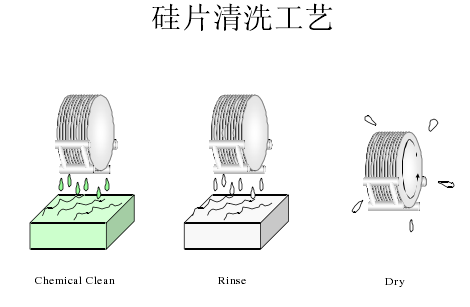
After cleaning, the wafer’s surface is dried to remove moisture, enhancing the adhesion of the photoresist to the surface, with typical drying temperatures around 100°C.
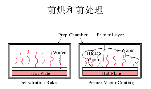
The wafer drying and pre-treatment prevent the photoresist from peeling off the wafer surface during development, and the dried wafer is cooled on a cooling plate.
(b) Spin Coating
The spin coating process involves attaching the wafer to a vacuum chuck, then dropping liquid photoresist in the center of the wafer, and as the chuck spins, the centrifugal force spreads the photoresist evenly across the wafer surface.
The image below shows the general structure of a spin coater and the spin coating process:
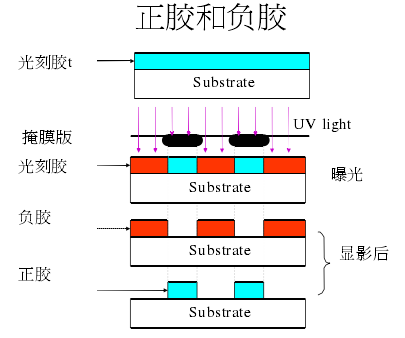

It is worth mentioning that photoresists can be classified into positive and negative resists. If we compare lithography to engraving text on a stone tablet, the text can be either raised or recessed. The positive and negative photoresists serve this function.

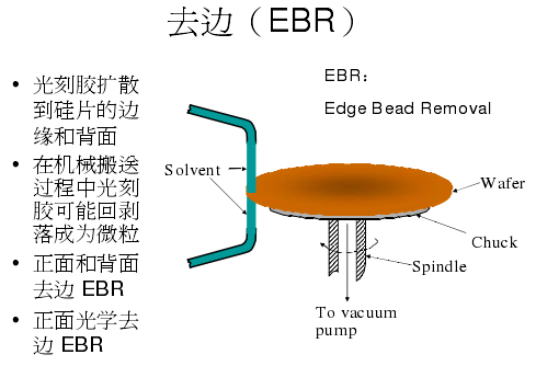
(c) Edge Bead Removal (EBR)
After coating the wafer, the photoresist may extend to the edges and back of the wafer, and during mechanical handling, the photoresist may peel off as particles.
The image below illustrates the edge bead removal process:
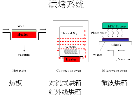
(d) Post-Coating Bake
The post-coating bake allows most of the solvent in the photoresist to evaporate.
The solvent in the photoresist helps achieve a thin photoresist film but absorbs light and affects adhesion.
The image below shows different baking equipment for wafers; regardless of the structure, the purpose remains the same, drying the wafer and photoresist like roasting sweet potatoes.
The baked wafer is then cooled on a cooling plate to ambient temperature.
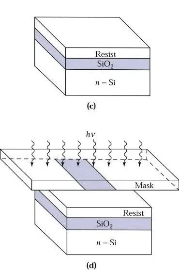
(e) Alignment and Exposure
Alignment and exposure are the essence of lithography.
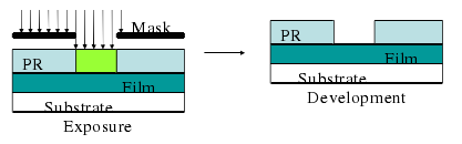
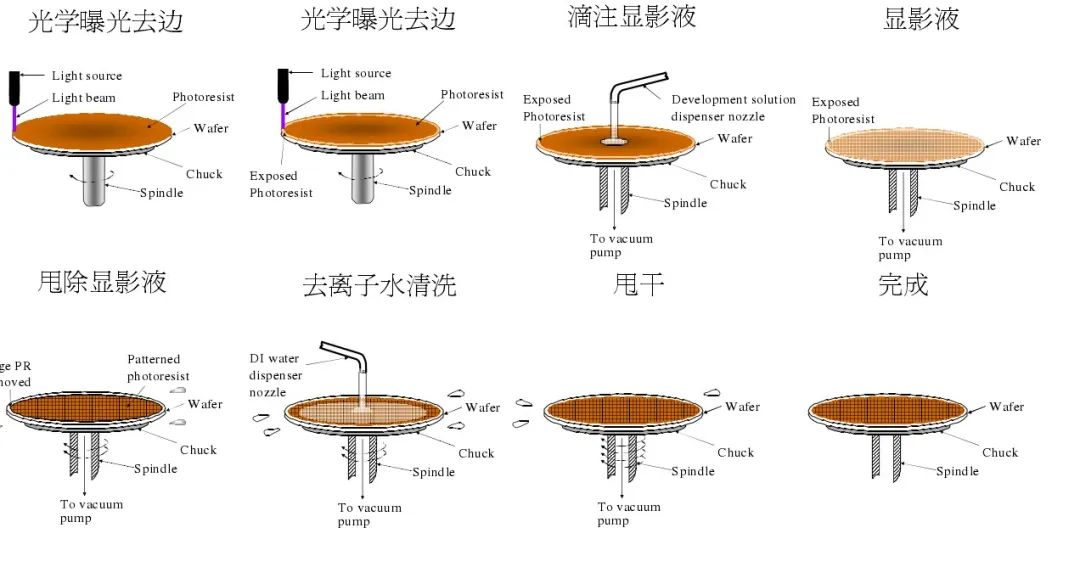
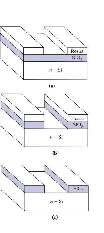
The lithography process uses a UV light source to expose the wafer through a patterned mask, as shown in the image below (d).
The areas of the wafer covered by the photoresist will chemically react according to the pattern of the photoresist, while the exposed photoresist will undergo polymerization reactions and will be difficult to remove in the etching solution. The polymer regions remain after the wafer is placed in the developer, while the unexposed areas (under the opaque mask regions) will dissolve and be washed away.
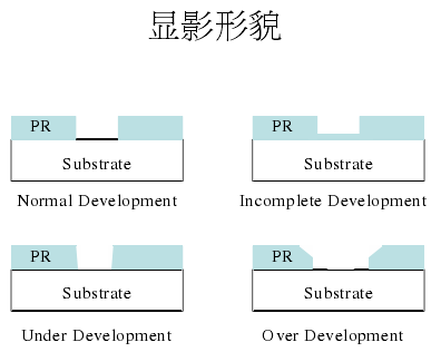
(f) Development
The development step after lithography involves using a developer to dissolve part of the photoresist; positive resists typically use a weak alkaline solvent, most commonly tetramethylammonium hydroxide, to transfer the pattern from the mask onto the photoresist.
The image below illustrates the lithography and development processes:
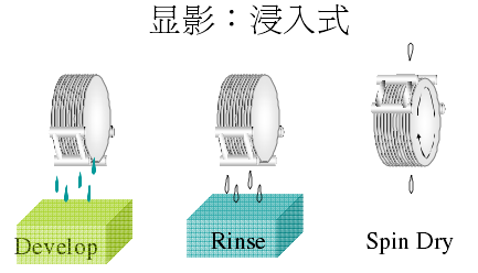
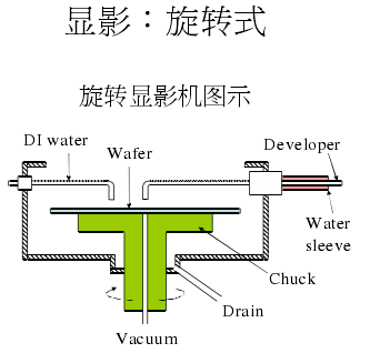
The development methods for silicon wafers are mainly divided into immersion and spray development.
Immersion involves placing the entire wafer in the developer.

With the completion of metallization, the p-n junction is now operational. After completing the above processes, a semiconductor P-N junction is formed, and through the above processes, devices such as Metal-Oxide-Semiconductor Field-Effect Transistors (MOSFETs) can be completed, allowing a simple semiconductor device to operate!
END
The reproduced content only represents the author’s views
It does not represent the position of the Institute of Semiconductors, Chinese Academy of Sciences
Editor: Schrödinger’s Cat
Editor-in-Chief: Fish for Three Dollars
Submission Email: [email protected]
1. The Semiconductor Institute has made progress in biomimetic covering neuron models and learning methods research.
2. The Semiconductor Institute has made significant progress in inverted structure perovskite solar cells.
3. Why is copper used as interconnect metal in chips?
4. What exactly is the 7nm technology in chips?
5. Silicon-based integrated photonic quantum chip technology.
6. How abnormal is the quantum anomalous Hall effect? It may bring about the next revolution in information technology!