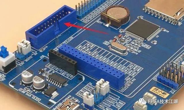
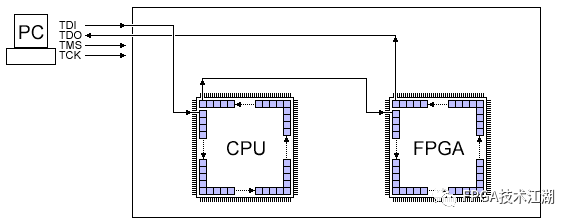
Originally published on the WeChat public account “Embedded Fun”.During the process of FPGA development and learning, a key step is programming the board, making hardware “hard reality” is crucial. Generally speaking, using the JTAG interface is quite common, so many experts must have encountered issues where the JTAG interface malfunctioned or was damaged and could not be used. Recently, I encountered such a situation where the JTAG interface of my FPGA suddenly could not download programs, and this was not the first time it happened. Previously, during a project, a similar issue occurred. It was working fine one day, and the next day it just wouldn’t work, which was quite frustrating. Therefore, I tried many solutions; initially, I did not consider that the JTAG interface could be broken. I replaced the USB Blaster, but there was no response at all. Could it really be that the JTAG interface was broken? Hence, I consulted relevant materials to understand the essence of the problem. Below are some of my findings that I share for everyone’s reference, hoping to exchange and learn together.Based on the materials I reviewed and my practical experience, during the use of the JTAG download interface, do not plug or unplug it while powered, as this may damage the JTAG signal pins of the FPGA chip. So how can you confirm if the JTAG interface is damaged? First, you need to rule out some basic factors: first, check if the connection is correct; many devices correspond to many interfaces, and you must match them correctly under actual conditions, otherwise, the above situation may occur. Second, rule out issues with the download cable; if the download cable is faulty, you can try using multiple cables to eliminate this type of problem. If you still cannot access the FPGA’s JTAG interface, it is very likely that the JTAG interface of your FPGA chip is damaged. At this point, please use a multimeter to check if TCK, TMS, TDO, and TDI are shorted to GND. If any signal is shorted to ground, it indicates that the JTAG signal pin is damaged.As for what the JTAG interface is, let’s discuss it here. JTAG stands for Joint Test Action Group.JTAG is an IEEE standard used to solve board-level issues, born in the 1980s. Today, JTAG is used for programming, debugging, and probing ports. Of course, the original use was for boundary testing.
1. Boundary Testing
For example, if you have two chips connected by many wires, how can you ensure that these connections are okay? By using JTAG, it can control all IC pins. This is called chip boundary testing.
2. JTAG Pins
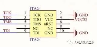
JTAG has developed to now and typically has four pins: TDI, TDO, TMS, TCK, and of course, a reset pin TRST. The JTAG pins on the chip are actually dedicated.
TDI: Test Data Input, data is input into the JTAG interface through TDI;
TDO: Test Data Output, data is output from the JTAG interface through TDO;
TMS: Test Mode Select, used to set the JTAG interface to a specific test mode;
TCK: Test Clock Input;
TRST: Test Reset.
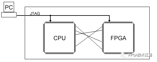
CPU and FPGA manufacturers allow JTAG to be used for port debugging; FPGA vendors allow configuration of FPGAs through JTAG, using JTAG signals to enter the FPGA core.
3. How JTAG Works
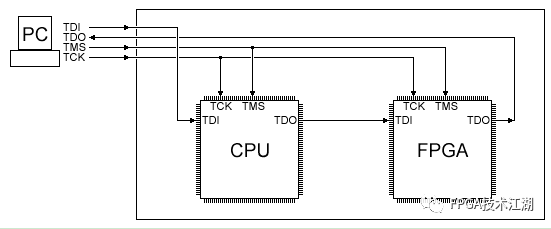
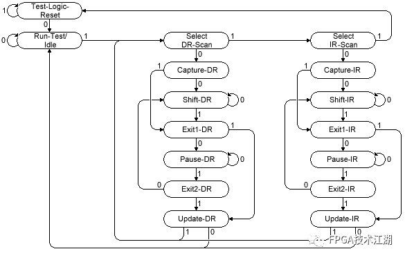
The PC controls JTAG: connect the JTAG cable to the PC’s printer port or USB or network port. The simplest is to connect to the printer port.TMS: Inside each chip with JTAG, there is a JTAG TAP controller. The TAP controller is a state machine with 16 states, and TMS is the control signal for it. When TMS connects each chip together, the TAP state transitions of all chips are consistent. Below is a diagram of the TAP controller:Changing the value of TMS will cause a state transition. If you keep a high level for 5 cycles, it will jump back to test-logic-reset, usually used to synchronize the TAP controller; the two most important states used are Shift-DR and Shift-IR, which connect TDI and TDO.IR: Instruction Register, you can write values to this register to tell JTAG to do something. Each TAP has only one IR register, and its length is fixed.DR: TAP can have multiple DR registers, similar to IR registers, each IR value selects a different DR register. (Very confusing)
4. JTAG Chain Related Questions
Calculating the number of ICs in the JTAG chain:An important application is that the IR value is all ones, indicating the BYPASS command. In BYPASS mode, the DR register in the TAP controller is always a single bit, from input TDI to output TDO, usually one cycle, doing nothing.You can use the BYPASS mode to calculate the number of ICs. If the delay of the TDI-TDO chain for each IC is one clock, we can send some data and detect how long it is delayed, then we can deduce the number of ICs in the JTAG chain.Obtaining the device ID in the JTAG chain:Most JTAG ICs support the IDCODE command. In the IDCODE command, the DR register will load a 32-bit value representing the device ID. Unlike the BYPASS instruction, there is no standard IR value in IDCODE mode. However, each time the TAP controller transitions to the Test-Logic-Reset state, it will enter IDCODE mode and load the IDCODE into DR.
5. Boundary Scan:
When the TAP controller enters boundary scan mode, the DR chain can traverse each IO block or read or intercept each pin. Using JTAG on an FPGA, you can know the state of each pin while the FPGA is running. You can use the JTAG command SAMPLE, though different ICs may have different implementations.If the JTAG interface is already damaged, then you can only “mourn the loss”. However, do not just be sad; the most important thing is to analyze the reasons behind it. The same principle applies to other matters. Let’s analyze it: during our usage, we might often plug and unplug the JTAG download interface casually for convenience. In most cases, this will not cause issues. However, there is still a small probability of the following problems occurring due to hot-plugging, resulting in static electricity and surges that ultimately lead to the breakdown of the FPGA pins. Additionally, there are suspicions about whether counterfeit USB Blasters or ByteBlasterII designs have simplified circuits by removing protective circuits, causing issues. However, feedback from many real situations has proven that original USB Blasters can also encounter the same problems. Some have questioned whether Altera’s low-end chips have not added diode clamping protection circuits to reduce costs for FPGA IO units. Such doubts do not address the essence of the problem. The most important thing is to standardize operations and minimize premature failure of hardware devices and interfaces due to improper handling. Now, the focus is on how we should standardize the use of the JTAG download interface.Power-on operation sequence:
1. With the FPGA development board and related devices powered off, connect the JTAG download cable;
2. Connect the USB Blaster or ByteBlasterII cable;
3. Power on the FPGA development board.
Power-off operation sequence:
1. Turn off the power to the FPGA development board and related devices;
2. Disconnect the USB Blaster or ByteBlasterII cable;
3. Disconnect the JTAG download cable and store it in a suitable place.
Although the above operation steps may seem cumbersome, and we may not pay much attention while using them, to ensure that the chip is not damaged, it is advisable to follow the steps as outlined. The issue I encountered was a short circuit between TCK and GND; although the probability of occurrence is not high, to use hardware-related devices more reasonably and for a longer time, I still recommend that everyone not worry about complexity and operate according to standard procedures. Thinking from another perspective, “more practice” is also beneficial for oneself. Finally, let me remind everyone that it is best not to hot-plug the JTAG download interface; at least it can help the JTAG interface “live” longer. After all, a long-term companion is quite nice; don’t wait until it’s gone to regret it.Source:FPGA Resource Knight