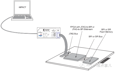
Xilinx‘s JTAG cable can directly program SPI/BPI. Many users who are not familiar with the Xilinx development environment may have questions when encountering this programming mode for the first time. How does the FPGA bridge between JTAG and Flash? Is there a dedicated circuit inside the FPGA to achieve this function?
Actually, no. The FPGA does not have a dedicated circuit designed (reserved) to convert JTAG to Flash. When we program the Flash via JTAG, the computer actually first downloads a bit file to the FPGA, and this temporary bit file serves as a bridge.
Therefore, the entire process of programming the flash is divided into 2 independent steps:
1. Pre-download a bit file to the target FPGA, establishing a bridge from JTAG to Flash.
2. Then, transfer the data to be programmed to the flash via JTAG.
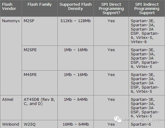
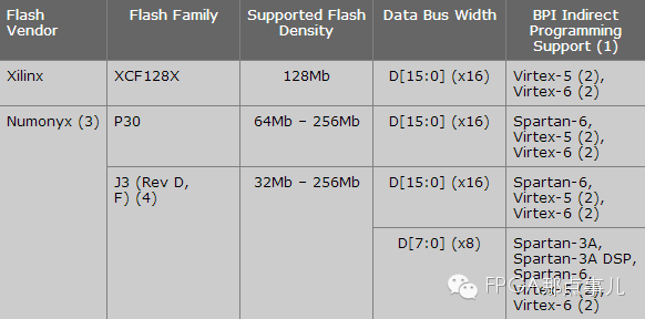
Since the pre-configured bit file cannot support all flash models, we need to pay attention to the list of models supported by Xilinx FPGA during the design selection:
SPI flash
BPI Flash
Note: The copyright belongs to the “FPGA That Matters” operation team, please indicate the source when reprinting.
Welcome to scan the QR code below to follow “FPGA That Matters”!