Background
In the previous section on hardware security, we used a programmer and UART debugging pins to extract the firmware from the Tenda AC6 router, mastering how to obtain firmware through the UART interface and gain terminal access for debugging analysis. Besides the commonly seen UART interface, we often encounter JTAG interfaces on PCB boards, which can also be used to extract firmware and perform debugging analysis. In this section, we will learn how to identify JTAG interfaces and conduct debugging analysis.
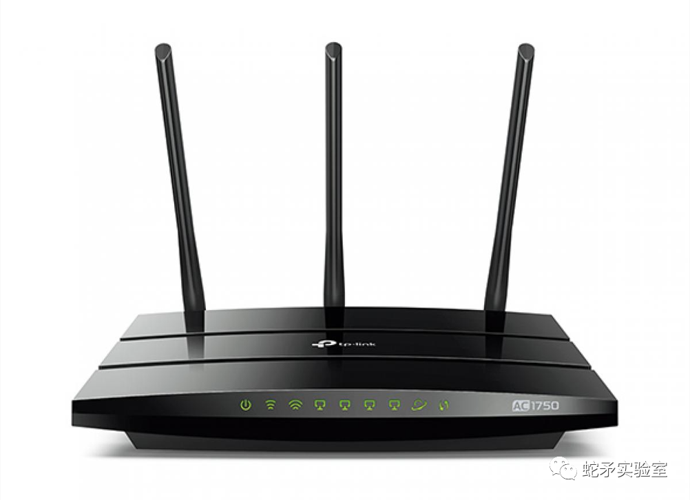
The hardware devices and tools needed for this section include: TP-Link Archer C7 router, Dupont wires, JTAGulator, and J-Link emulator.
JTAG Basics
Definition of JTAG


JTAG stands for Joint Test Action Group, which is a commonly used name for the IEEE standard 1149.1, known as the Standard Test Access Port and Boundary Scan Architecture. This standard is used to verify the functionality of printed circuit boards produced through design and testing. JTAG was officially standardized in 1990 by IEEE document 1149.1-1990, and in 1994, a supplementary document was added to explain the Boundary Scan Description Language (BSDL). Since then, this standard has been widely adopted by electronic companies worldwide. Boundary scan has almost become synonymous with JTAG. In the design of printed circuit boards, it is mainly used for testing integrated circuit sub-blocks and also provides a useful debugging mechanism for embedded systems, offering a convenient “backdoor” in the system. When using debugging tools like in-circuit emulators, JTAG serves as the mechanism for signal transmission, allowing programmers to read debugging modules embedded in the CPU through JTAG. The debugging module enables programmers to debug software within embedded systems.
In simple terms, JTAG is not a communication protocol like UART, even though the specific manifestations are pin interfaces that we can see on PCB boards. JTAG is a method for testing and debugging device chips and utilizes boundary scan technology (Boundary scan refers to sending data to the chip and matching outputs with inputs to verify whether the chip is functioning correctly. I understand this as a brute-force cracking method at the hardware level, but not a single-point state cracking, rather a chain cracking method). The basic principle of JTAG is to define a TAP (Test Access Port) inside the device and test internal nodes using specialized JTAG testing tools. JTAG testing allows multiple devices to be chained together through the JTAG interface, enabling individual testing of each device. For beginners, we do not need to focus on how JTAG is implemented (https://www.fpga4fun.com/JTAG2.html), we just need to know a few functions of JTAG, which are:
1. Download and programming, allowing programming of flash chips.

2. Debugging, allowing debugging analysis of chips and peripheral devices.

3. Chip pin diagnostics, allowing testing of the status of various chip pins.
Common JTAG Pin Arrangements
In practical applications, different IC companies define their proprietary JTAG connectors. In embedded systems, common JTAG connectors include 10PIN, 14PIN, 16PIN, and 20PIN with the following pin arrangements:
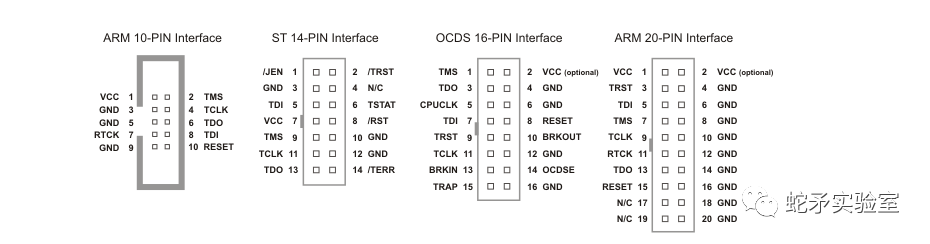
Note: The above diagram only shows common JTAG arrangements, and specific instances require specific analysis.
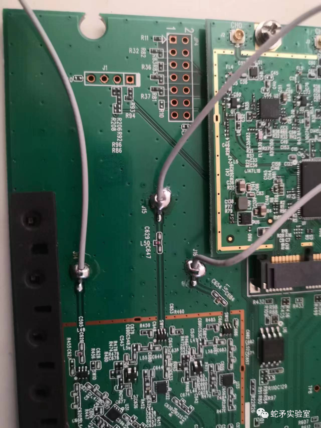
In the PCB board of the TP-Link Archer C7 router, we see a single-row 4-pin interface and a double-row 14-pin interface in the lower left corner. Testing shows that the 4 pins are UART interfaces, while the 14 pins are JTAG interfaces. Next, we will focus on identifying the JTAG pins and connecting the J-Link emulator for debugging analysis.
Identifying JTAG Pins
Using JTAGulator
JTAGulator (http://www.grandideastudio.com/portfolio/jtagulator/) is an open-source hardware tool that mainly features automatic interface identification, logic analysis, and programming capabilities. It is an excellent hardware security device, very suitable for people learning hardware security. JTAGulator can be purchased on various platforms or printed by oneself. A domestic JTAGulator user manual is available (https://www.bilibili.com/read/cv13047230).
Identifying UART Pins with JTAGulator
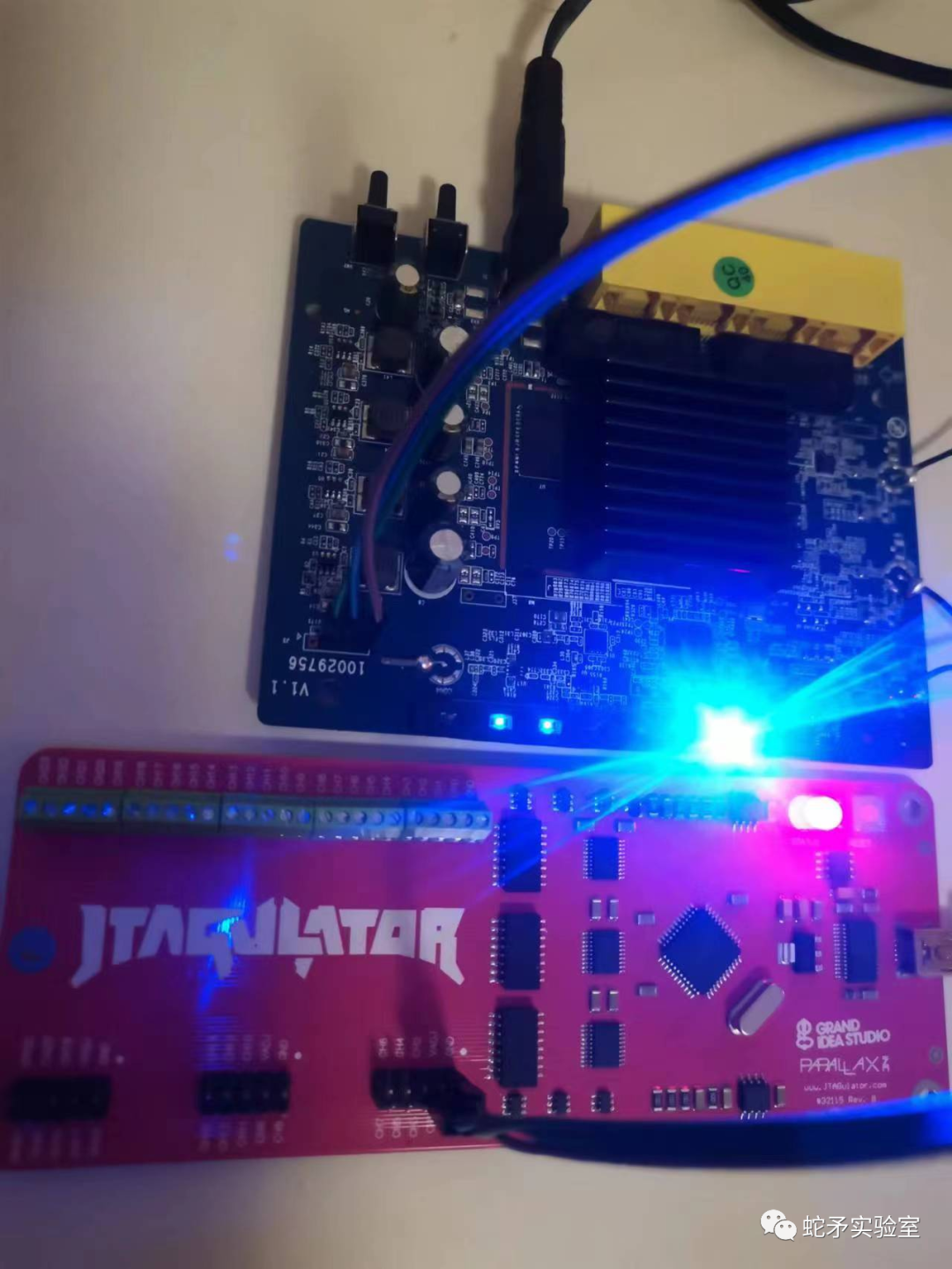
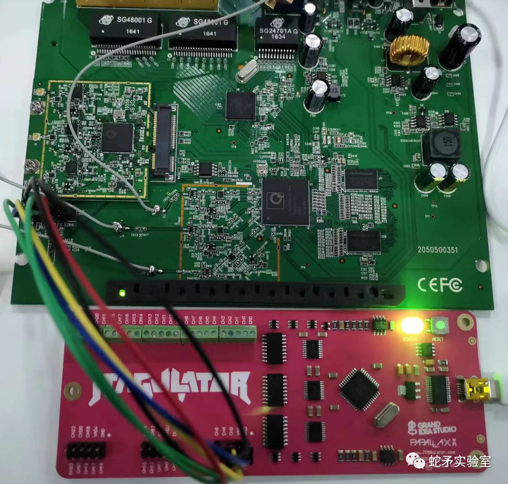
Taking the previous section’s Tenda AC6 router UART pin identification as an example, before using JTAGulator, we need to manually identify the GND pin (the method for identifying the GND pin can be found in the previous section). After identifying the GND pin, we connect several pins from the router (excluding GND) to JTAGulator’s channel 0, 1, 2, and then connect the router’s GND pin to JTAGulator’s channel GND. Next, we power on the router and connect JTAGulator’s USB to our PC.
We need to open a terminal simulation software on our computer (here I use SecureCRT), connect via serial port, set the baud rate to 115200, and after clicking connect, press enter to see the JTAGulator banner. By entering the ‘h’ command, we can view the command help for JTAGulator. The ‘j’ command is for JTAG mode, allowing a series of operations on the JTAG interface, such as scanning JTAG pins and connecting to OpenOCD. The ‘u’ command is for entering UART mode, allowing a series of operations on the UART interface, such as scanning UART pins and using the UART interface for debugging. Similarly, the ‘G’ command (GPIO interface) and ‘S’ command (SWD interface) correspond to their respective modes.
Before entering the corresponding mode, we need to use the ‘v’ command to set the device voltage, usually set to 3.3V.
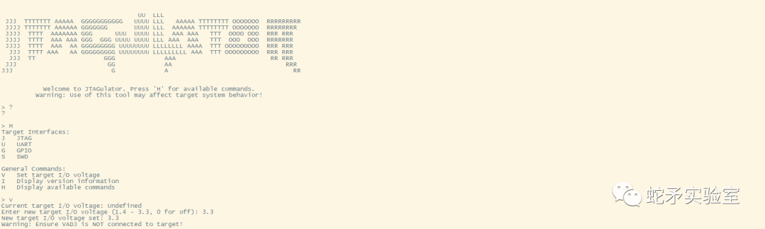
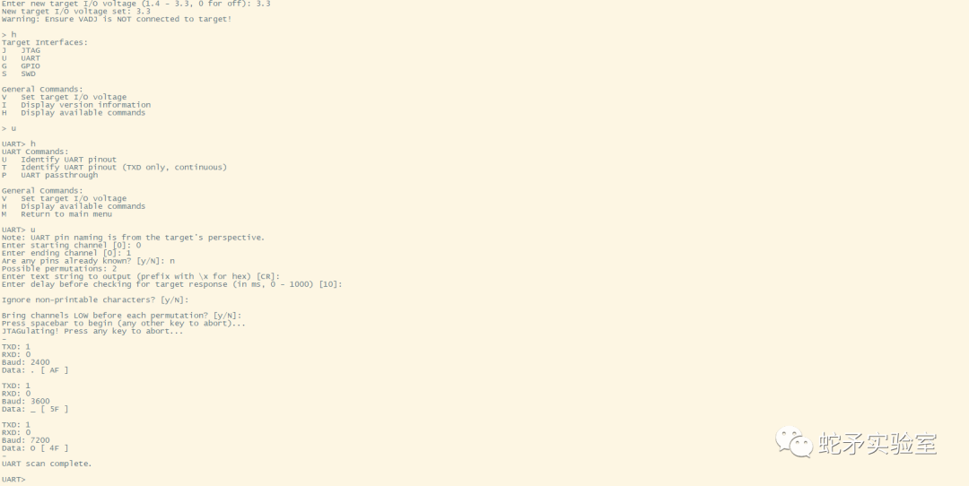
After setting the voltage, we enter ‘u’ to enter UART mode. After viewing the help commands, we can use ‘u’ to scan UART pins, and the ‘T’ command scans only the TX pin. The ‘P’ command uses the UART pin to enter the terminal. We use the ‘u’ command to start scanning pins, which requires setting the start channel and end channel before proceeding with default settings. Pressing the space key starts the scan, and after a moment, JTAGulator will print the pin information. As shown in the figure, the TX pin is channel 1, and the RX pin is channel 0. The baud rate provided by JTAGulator is guessed after scanning visible characters, and since they are all special symbols, the displayed baud rate may not be very accurate.
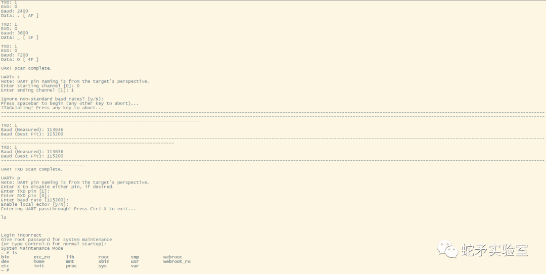
We can continue using the ‘t’ command to scan the TX pin to verify the previous scan results. The result shows that the TX pin is indeed channel 1, and it also scanned a baud rate of 115200. Using the ‘p’ command, we enter the terminal for testing (here we directly use the default parameters scanned by JTAGulator), set the parameters, and input the password analyzed in the previous section to log in, successfully entering the terminal.
Identifying JTAG Pins with JTAGulator
First, use a multimeter to test the GND pin of the TP-Link Archer C7 router (the method has been explained in the previous section), then connect the other pins to the channels on JTAGulator.
Using SecureCRT to connect, input ‘j’ to enter JTAG mode and check the help commands. The ‘j’, ‘i’, and ‘b’ commands are all used for scanning JTAG pins, with ‘j’ and ‘i’ being faster, and ‘b’ being slower. The ‘r’ command can identify the RTCK pin, the ‘d’ command retrieves the device ID number, ‘t’ is for bypass testing, ‘y’ is for instruction/data register testing, ‘p’ is for port mapping, and ‘o’ is for OpenOCD interface mode.
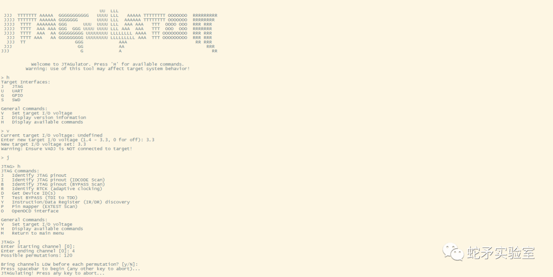
Using the ‘j’ command to scan, we similarly need to set the start channel and end channel before proceeding with default settings. Pressing the space key starts the scan, and after a moment, JTAGulator scans several JTAG interfaces, with channel 1 being TDI, channel 2 being TDO, channel 4 being TCK, and channel 3 being TMS. Sometimes, running only the ‘j’, ‘i’, or ‘b’ commands may not yield results, so we can run all three commands to confirm.
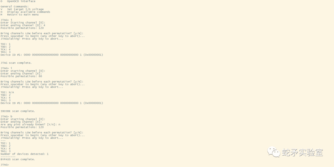
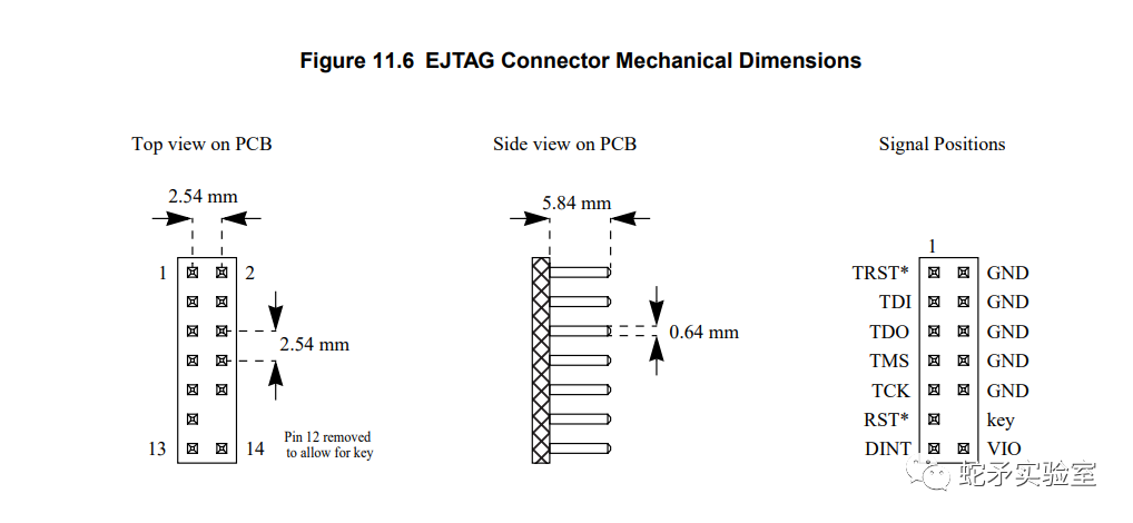
We have determined the TCK, TMS, TDO, TDI, and GND pins of the router through JTAGulator. If we want to use the JTAG interface for debugging, we also need to use a multimeter to find the VIO pin. After powering on the router, we identified the VIO pin by checking the pin voltage or shorting methods. The pin distribution is shown in the figure below:
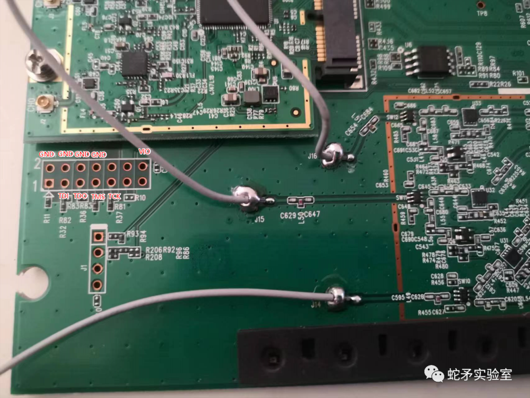
All the JTAG pins required for debugging have been identified, and we just need to connect them to the corresponding pins of the J-Link for debugging.
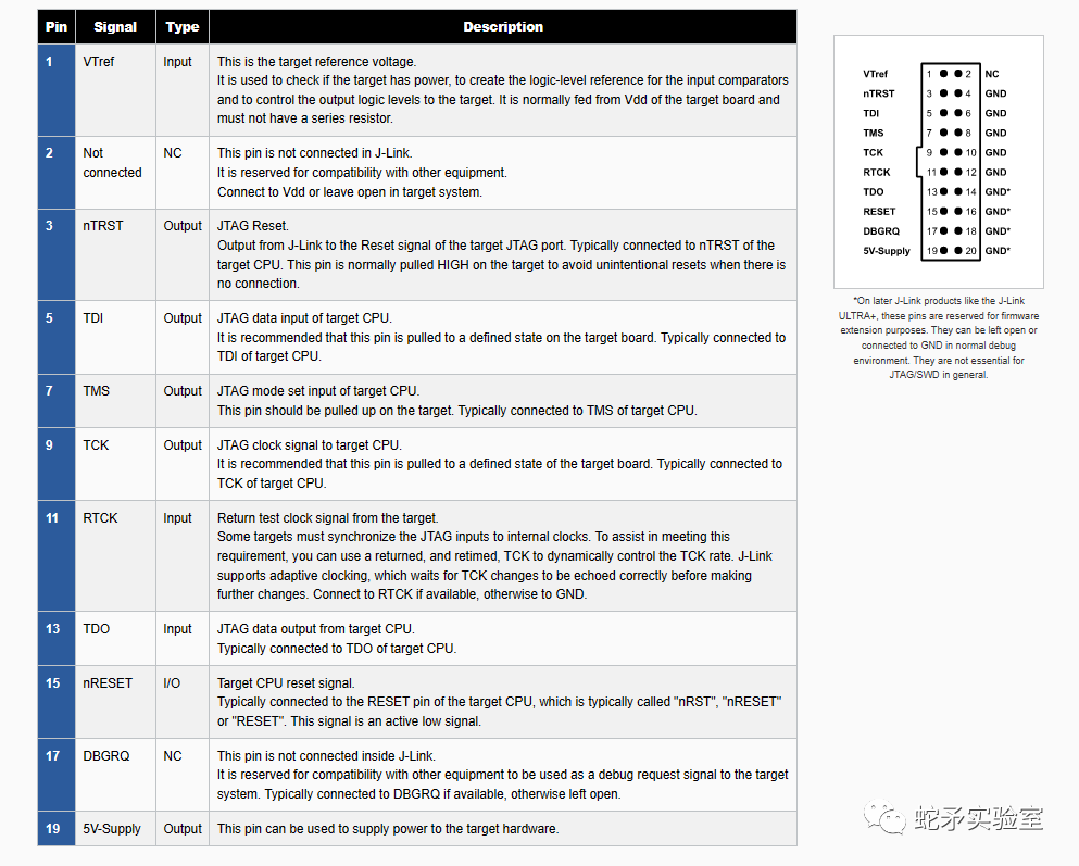
If we want to add additional options during debugging, we need to know the definitions of all 14 pins of JTAG in the router, which requires us to find information based on the analyzed pins and chip models.
JTAG Debugging Analysis
The J-Link can debug MCUs using its built-in drivers, but since J-Link does not support many device models by default (for example, the QCA95xx in this section), we need to use OpenOCD.
OpenOCD (Open On-Chip Debugger) is an open-source on-chip debugger, initially started as a project by Dominic Rath during university (2005). OpenOCD aims to provide debugging, system programming, and boundary scan functions for embedded devices.
In the previous domestic JTAGulator user manual link and the later content on the ath79 configuration file, detailed explanations on how to install and debug OpenOCD on Linux are provided, so I will not demonstrate it here. The debugging process on Windows is roughly the same, and I will now use Windows to install OpenOCD for debugging analysis.
-
First, we need a J-Link emulator, which costs around 100 yuan on various platforms. Install the J-Link driver software provided by the vendor or download it from the SEGGER website. Download the OpenOCD Windows compressed package (https://gnutoolchains.com/arm-eabi/openocd/), extract it, and place the bin directory in the environment variable. At this point, OpenOCD is installed.
-
OpenOCD needs to use J-Link to debug the MCU. Here, OpenOCD requires J-Link to be used as a regular USB device, so we need to replace the default J-Link driver. To do this, download the Zadig tool (https://zadig.akeo.ie/) and run it, go to the “Options” menu, and select “List All Devices”. Check the device list, select the corresponding J-Link driver, and then click “Replace Driver”. At this point, the driver is also installed.
-
Proceed with the debugging process.
Common OpenOCD Commands
poll: Query the current status of the target board
halt: Interrupt the operation of the target board
resume [address]: Resume the operation of the target board, starting from the specified address if provided
step [address]: Step through execution, starting from the specified address if provided
reset: Reset the target board
mdw <Addr> [Count]: Display Count (default is 1) words (4Bytes) starting from address Addr
mdh <Addr> [Count]: Display Count (default is 1) half-words (2Bytes) starting from address Addr
mdb <Addr> [Count]: Display Count (default is 1) bytes (1Byte) starting from address Addr
mww <Addr> <Value>: Write Value to address Addr, size: one word (4Bytes)
mwh <Addr> <Value>: Write Value to address Addr, size: one half-word (2Bytes)
mwb <Addr> <Value>: Write Value to address Addr, size: one byte (1Bytes)
load_image <file> <address> ["bin"|"ihex"|"elf"]: Load file <file> into memory at address <address>, formats include "bin", "ihex", "elf"
dump_image <file> <address> <size>: Read size bytes of data starting from address and save to file <file>
After connecting the router’s TCK, TMS, TDO, TDI, GND, TRST, and VIO pins to the J-Link’s TCK, TMS, TDO, TDI, GND, nTRST, and VTref interfaces, connect the J-Link’s USB interface to the computer.
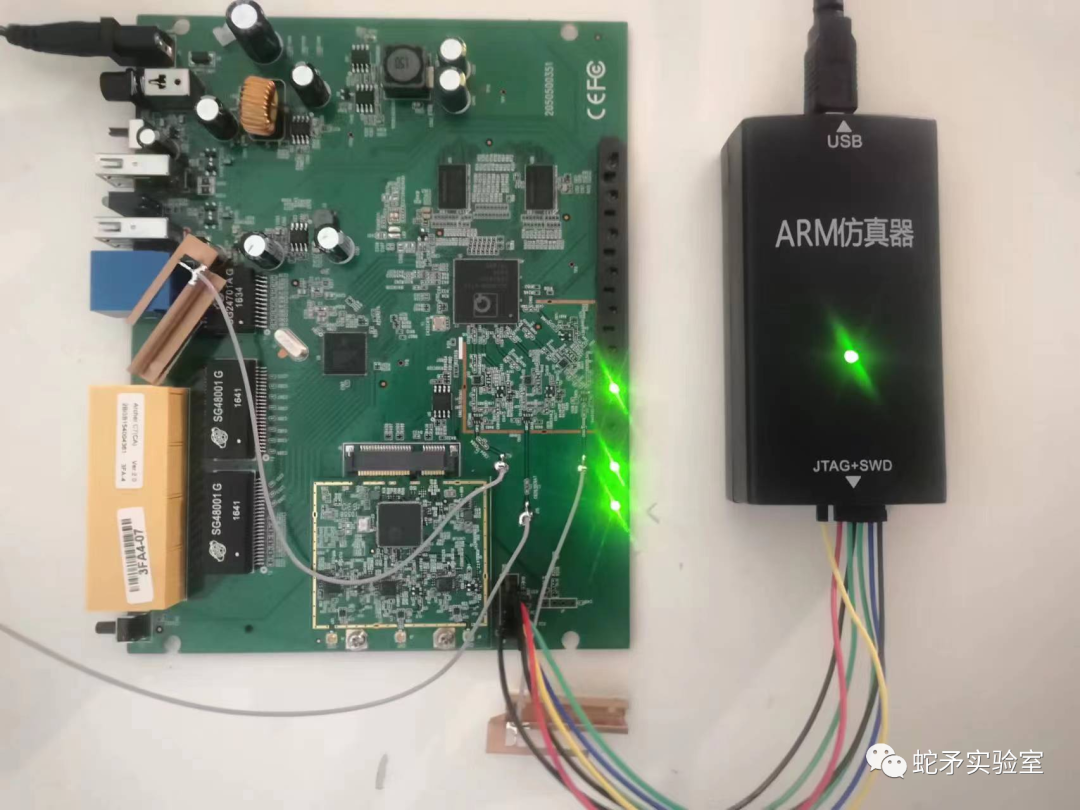
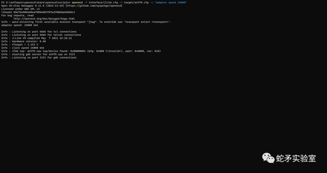
Before starting OpenOCD for debugging, we need to confirm the OpenOCD emulator configuration file and target device configuration file. Since we are using the J-Link emulator, the configuration file is jlink.cfg (openocd/share/openocd/scripts/interface/jlink.cfg). The selection of the target device configuration file needs to be based on the TP-Link Archer C7 SoC model (QCA9558-AT4A). After researching, we found that we should use the ath79 configuration file for OpenOCD debugging (https://openwrt.org/docs/guide-user/hardware/debrick.ath79.using.jtag#ath79cfg), and we will copy ath79.cfg to the openocd/share/openocd/scripts/target directory.

Using openocd -f interface/jlink.cfg -f target/ath79.cfg -c “adapter speed 15000” to run the debugging process. Once connected successfully, we can use GDB to connect to port 3333 for debugging, port 4444 can be connected using telnet, and tcl can connect to port 6666.
Note: “-f interface/jlink.cfg” specifies the emulator configuration file, “-f target/ath79.cfg” specifies the target configuration file, and “-c “adapter speed 15000″” executes the adapter speed command.
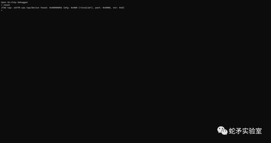
We open a terminal and use telnet to connect to localhost on port 4444. After a successful connection, we can use the reset command to reset the target board, at which point we find that the device returns 0x00000001, confirming that we are connected. We can also start GDB using target remote localhost:3333 for dynamic debugging (OpenOCD prompts us to use target extended-remote localhost:3333).
The halt command interrupts the target board’s operation, and the reset init command initializes the ath79.cfg configuration file.
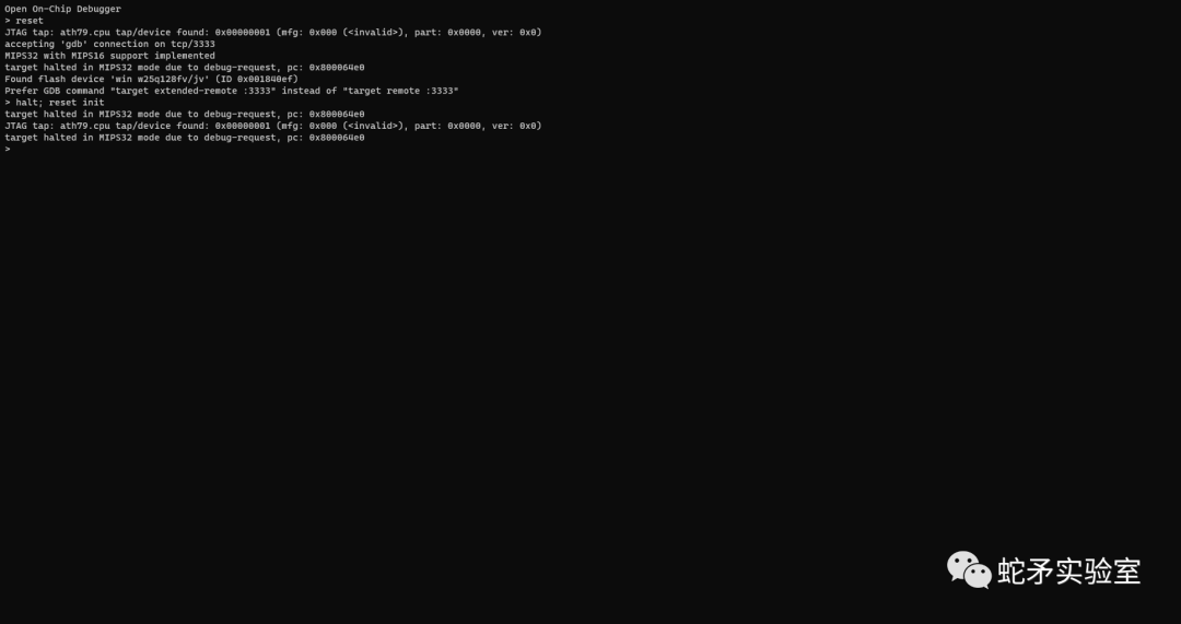
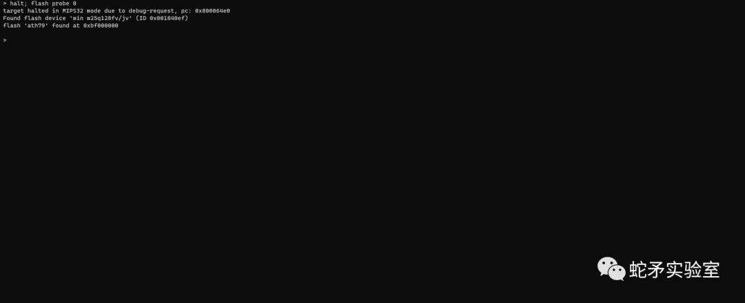
Using the flash banks command lists flash configuration information. Based on the index number, we use the flash probe 0 command to detect the identifier and related parameters of the flash chip, which turns out to be win w25q128fv/jv. Comparing with the Archer C7 router’s flash chip, we find it consistent, indicating that OpenOCD has detected correctly, and it shows the flash address as 0xbf000000.
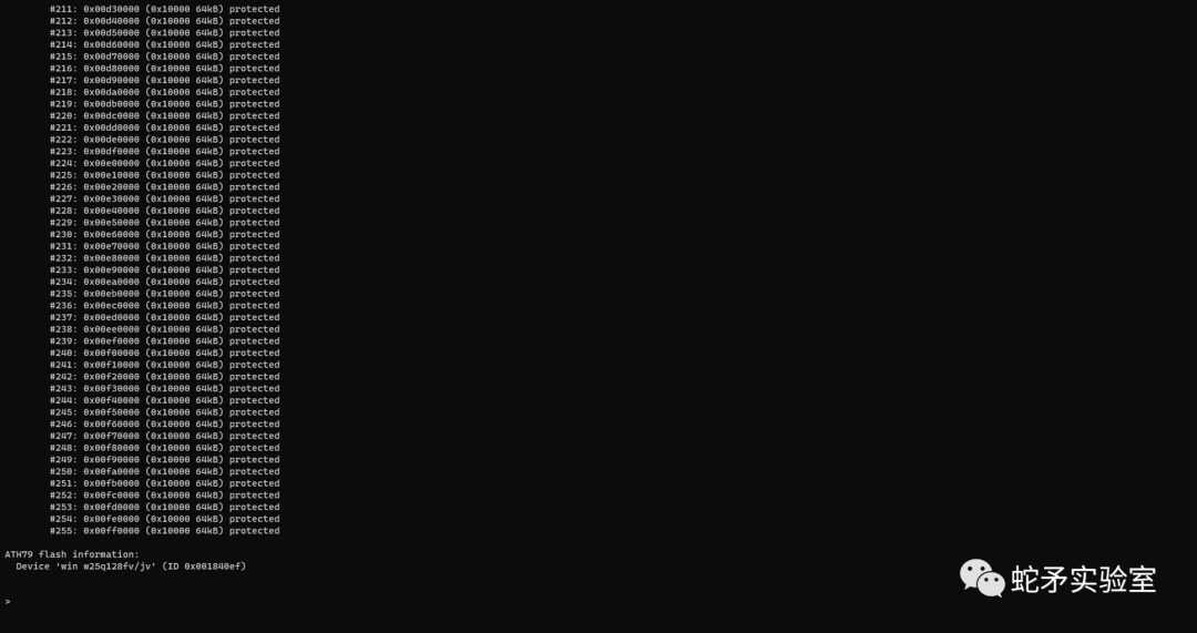
Using the flash info 0 command, we can view the memory distribution of the flash chip.
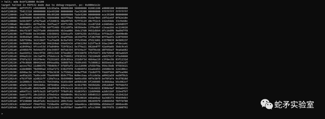
We can use the mdw <addr> [count] command to view the contents of the flash memory (the value 687173 in the figure is the squashfs magic header) and use the dump_image firmware.bin 0xbf000000 0x1000000 command to export the flash memory. Subsequently, we can analyze the firmware and dig for vulnerabilities.
Conclusion
In this section, we briefly learned how to use the JTAGulator tool, how to identify JTAG pins, and how to connect JTAG pins to the emulator for debugging analysis. This knowledge will also be very helpful when we later use testing hooks to extract debugging pins JTAG/SWD from the MCU and extract firmware.

Zhangan Network Security Spearhead Laboratory was established in 2020, dedicated to security research, offensive and defensive solutions, target field benchmarking scenario simulation, and technical and tactical design and output. The core members of the team are all security experts with over 10 years of experience in the security industry, currently involved in red-blue confrontation, penetration testing, reverse cracking, virus analysis, industrial control security, and evasion techniques.