In 1985, European manufacturing organizations established the Joint European Test Action Group (JETAG) to research testing for integrated circuits. Later, in collaboration with North American companies, this organization was renamed JTAG (Joint Test Action Group) in 1986, and corresponding testing standards were designated. This standard was approved by IEEE in 1990 as an international standard testing protocol IEEE1149.1-1990, which is the Test Access Port and Boundary Scan Architecture standard. This standard specifies the hardware and software required for boundary scanning. Since its approval in 1990, IEEE has made supplementary updates to this standard in 1993 and 1995, forming the currently used IEEE1149.1a-1993 and IEEE1149.1b-1994.
JTAG generally has three main functions:
• Downloader: We know that the signals on the pins of the chip communicating with the outside world are merely data and control signals. All of these signals pass through the CPU’s scan chain, and it is thus possible to inject program code into the corresponding storage medium through the scan chain’s TDI in a certain mode, enabling program downloading and debugging;
• DEBUG;
• Boundary Scan: Chips interact with peripheral devices through pins, and all data enters the chip through these pins. By inserting a scan chain inside the chip, monitoring pin signals can be achieved;
Therefore, JTAG is primarily applied in actual engineering for: circuit boundary scan testing, ISP (In-System Programmable, online programming), and for FLASH boundary operations (traditionally, chips are pre-bound before being mounted on boards). Initially, it was used for boundary testing. Generally, each chip has a TAP (Test Access Port) controller (which implements a state machine; the structure of this state machine is shown in the figure below), and JTAG test stimuli control TAP transitions through the TMS signal, completing corresponding operations and generating required control signals in different states.
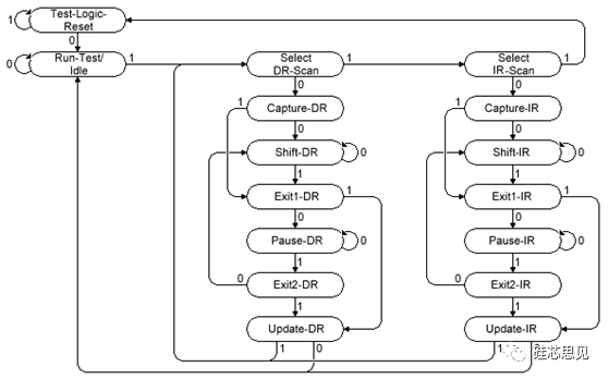
JTAG testing tools generally interact with the TAP controller through the following main interfaces:
TCK (Test Clock) — Test clock input; this test clock is independent, so the original functional clock is irrelevant;
TDI (Test Data In) — Test data input; data is input into the JTAG port via TDI, and the input data can generally be of two types: one is instruction signals sent to the instruction register, and the other is test data input into the corresponding boundary scan register;
TDO (Test Data Out) — Test data output; data is output from the JTAG port via TDO, and the output data can be of two types: one is instructions shifted out from the instruction register, and the other is data shifted out from the boundary scan register;
TMS (Test Mode Select) — Test mode selection; TMS is used to set the JTAG port to a specific test mode, generally sampled on the rising edge of TCK;
Optional pin TRST — Test reset, input pin, active low.
The general JTAG structure is as follows:
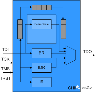
In the TAP controller’s state machine, DR refers to the Data Register and IR refers to the Instruction Register, which mainly implements operations such as instruction execution, decoding, and latching. Each TAP controller has one IR, but can have multiple DR registers.
The IR register consists of a shift register and a latch, with a length equal to that of the instruction. The IR connects between TDI and TDO, with instructions serially input from TDI while being latched in the latch. It is important to note that because JTAG has three mandatory commands (EXTEST, BYPASS, SAMPLE/PERIOD), the width of this register must be at least 2 bits.
The DR register is similar to the IR; different instructions processed in the IR register generally correspond to different DR registers.
The BR register is connected between TDI and TDO like the IR register; this register has a width of 1 bit, providing the minimum serial channel between TDI and TDO;
The IDR register is a 32-bit register, and its content generally includes information about the device’s version number, model, manufacturer, etc. This register can be queried when the device needs to be replaced;
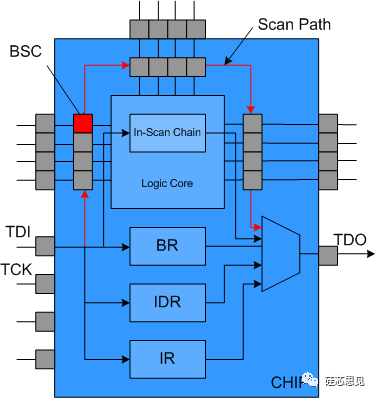
The Boundary Scan Register (BSR) consists of all boundary scan cells (BSC) on the device pins, which are connected in series to form a JTAG loop inside the IC. All BSR boundary scan registers are activated by JTAG testing, and these pins maintain normal IC functionality during regular operation. The path is shown in the figure below:
🎉🎉🎉🎉🎉🎉🎉🎉🎉🎉🎉🎉🎉🎉🎉🎉🎉🎉🎉
Knowledge is invaluable, and I hope this is helpful to you!
This article is for learning purposes only; please feel free to point out any shortcomings in the text. If the cover image infringes any rights, please communicate promptly!

Recommended good books are as follows!