In the previous article “UART Communication Interface Protocol – UART (I) Protocol Basics”, we briefly and meticulously describedUART configuration items and the signal timing of the communication process. This article will continue to introduce some interface specifications used by theUART interface under different electrical characteristics.
1. Introduction
In fact,UART only defines the signal timing without specifying its electrical characteristics. In different application scenarios, varying wiring spaces, and harsh environments with different levels of interference, usingUART for communication, the differences in electrical characteristics of the signal pins present a significant obstacle. Furthermore, many low-power devices generally operate at lower signal levels (less than 5V). Therefore, it is necessary to establish different electrical characteristic protocols to accommodate various application scenarios and environments.
2. UART Interfaces Under Different Electrical Standards
For different platforms or usage environments, the electrical characteristics of the signal pins can be classified as follows:
TTL/CMOS, RS232, RS422, RS485.
(1) TTL/CMOS
TTL level, logic “0” equals 0V voltage, logic “1” equals +5V voltage.
CMOS level, logic “0” is close to 0V voltage, logic “1” is close to the supply voltage (3.3V or others).
Comparison of TTL and CMOS Circuits
1) TTL circuits are current-controlled devices, while CMOS circuits are voltage-controlled devices.
2) TTL circuits are faster with shorter transmission delay times(5-10ns), but consume more power.
CMOS circuits are slower with longer transmission delay times(25-50ns), but consume less power.
CMOS circuit power consumption is related to the input signal pulse frequency; the higher the frequency, the hotter the chip, which is normal.
Commonly, in embedded development, theUART signal level is determined by theMCU chip.
In daily development, the MCU pin’s UART communication level is TTL/CMOS level signal.
(2) RS-232
RS232 stands for EIA-RS-232C standard, where EIA is the Electronic Industry Association representing the American Electronic Industry Association, RS is the Recommended Standard indicating the recommended standard, 232 is the identification number, and C indicates the third revision.
It was established in 1970 by the American Electronic Industry Association (EIA) in collaboration with Bell Systems, modem manufacturers, and computer terminal manufacturers as a standard for serial communication.
Thus, RS232 is the ancestor of UART!
RS232 specifies the electrical characteristics, logic levels, and various signal line functions.
On the TxD and RxD signal pins:
Logic “1” voltage range -3V~-15V
Logic “0” voltage range +3~+15V
On the RTS, CTS, DSR, DTR, and DCD control lines:
Signal valid (ON state, positive voltage) voltage range +3V~+15V
Signal invalid (OFF state, negative voltage) voltage range -3V~-15V
It can be seen that the signal pin characteristics of RS232 are characterized by negative logic levels.
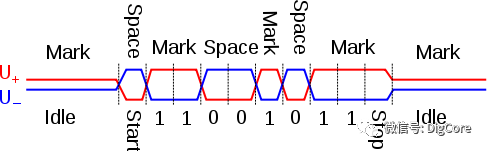
Specific observations can be made from the following data waveform of the MAX232 chip:
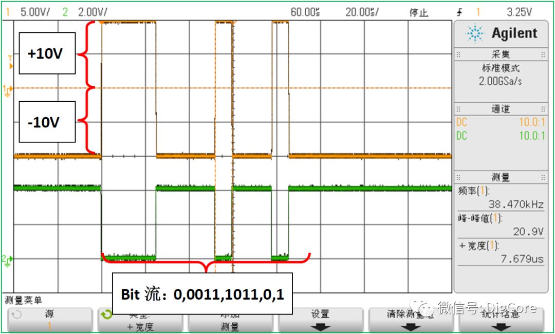
In the oscilloscope screenshot above, channel 1 (orange) represents the RS232 level, while channel 2 (green) represents the UART level.
Channel 2’s waveform corresponds to the bit stream of the data output level by level.
The bit stream consists of the start bit “0”, data “0011,1011” (which is the binary representation of the DigCore flag 0xDC in LSB order), odd parity bit “0”, stop bit “1”, with the pin ultimately in a high-level idle state.
In contrast, the negative logic level of RS232 has not only opposite signals but also different voltage levels.
On the MAX232 chip, logic “0” corresponds to +10V, while logic “1” corresponds to -10V.
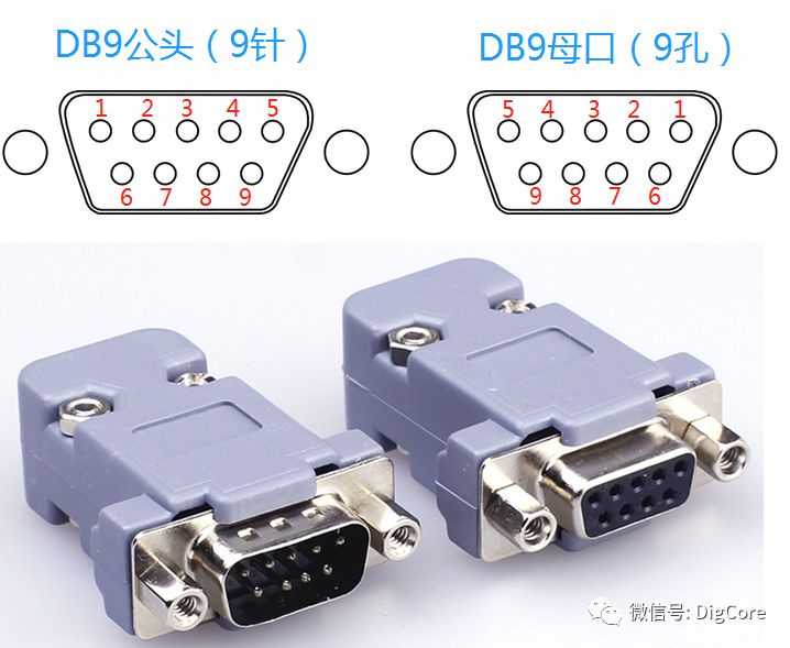
RS232 also defines mechanical interface characteristics, commonly including the DB-9 and DB-25 interfaces, with the following interface definitions:
|
Pin |
Signal |
Definition |
Function |
|
|
DB-9 |
1 |
DCD |
Carrier Detect |
Data Carrier Detect |
|
2 |
RXD |
Receive Data |
Received Data |
|
|
3 |
TXD |
Transmit Data |
Transmit Data |
|
|
4 |
DTR |
Data Terminal Ready |
Data Terminal Ready |
|
|
5 |
SGND |
Signal Ground |
Signal Ground |
|
|
6 |
DSR |
Data Set Ready |
Data Set Ready |
|
|
7 |
RTS |
Request to Send |
Request To Send |
|
|
8 |
CTS |
Clear To Send |
Clear To Send |
|
|
9 |
RI |
Ring Indicator |
Ring Indicator |
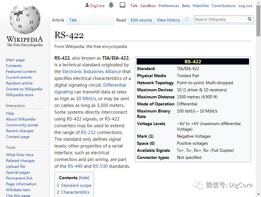
(3) RS-422
RS-422 stands for “Balanced Voltage Digital Interface Circuit Electrical Characteristics”, which defines the electrical characteristics of the interface circuit.
Except for the electrical characteristics of the signal lines, other specifications are essentially derived from RS232 standards.
RS-422 uses a differential transmission method for the signal lines, meaning that the original TxD and RxD signal lines are replaced by two wires, namely TxD+ and TxD-, and RxD+ and RxD-, utilizing the voltage difference between the two wires to represent data logic“1” and logic “0”.
Logic “1” differential signal voltage difference range: +2~+6V
Logic “0” differential signal voltage difference range: -6~-2V
Maximum communication distance: 1500 meters
Communication rate range: 100 kbit / s – 10 Mbit / s
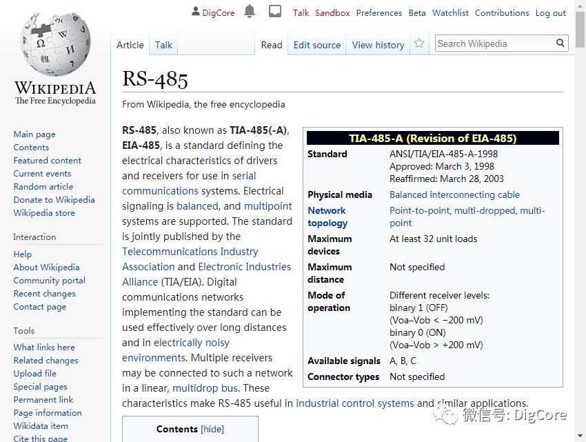
(4) RS-485
EIA developed the RS-485 standard in 1983 based on RS-422, changing from 4 lines to 2 lines for transmission, thus converting full duplex to half duplex and increasing multipoint, bidirectional communication capabilities.
Two-wire half duplex only uses 2 differential lines A and B for connection, where A line’s “high” represents logic “0” and low represents logic “1”; B line’s “high” represents logic “1”, while “low” represents logic “0”.
A diagram can clarify this; the following image is a timing diagram from the Wikipedia page on RS485:
References:
Wikipedia UART:
https://en.wikipedia.org/wiki/Universal_asynchronous_receiver-transmitter
Wikipedia RS-482:
https://en.wikipedia.org/wiki/RS-422
Wikipedia RS-485:
https://en.wikipedia.org/wiki/RS-485


www.digcore.cn
More technical content awaits you!
Long press the QR code to follow