Name: UART Asynchronous Serial Communication Circuit Design Verilog Code for Quartus FPGA_C4_V2.1 Experimental Board
Software: Quartus
Language: Verilog
Code Function:
Function Description
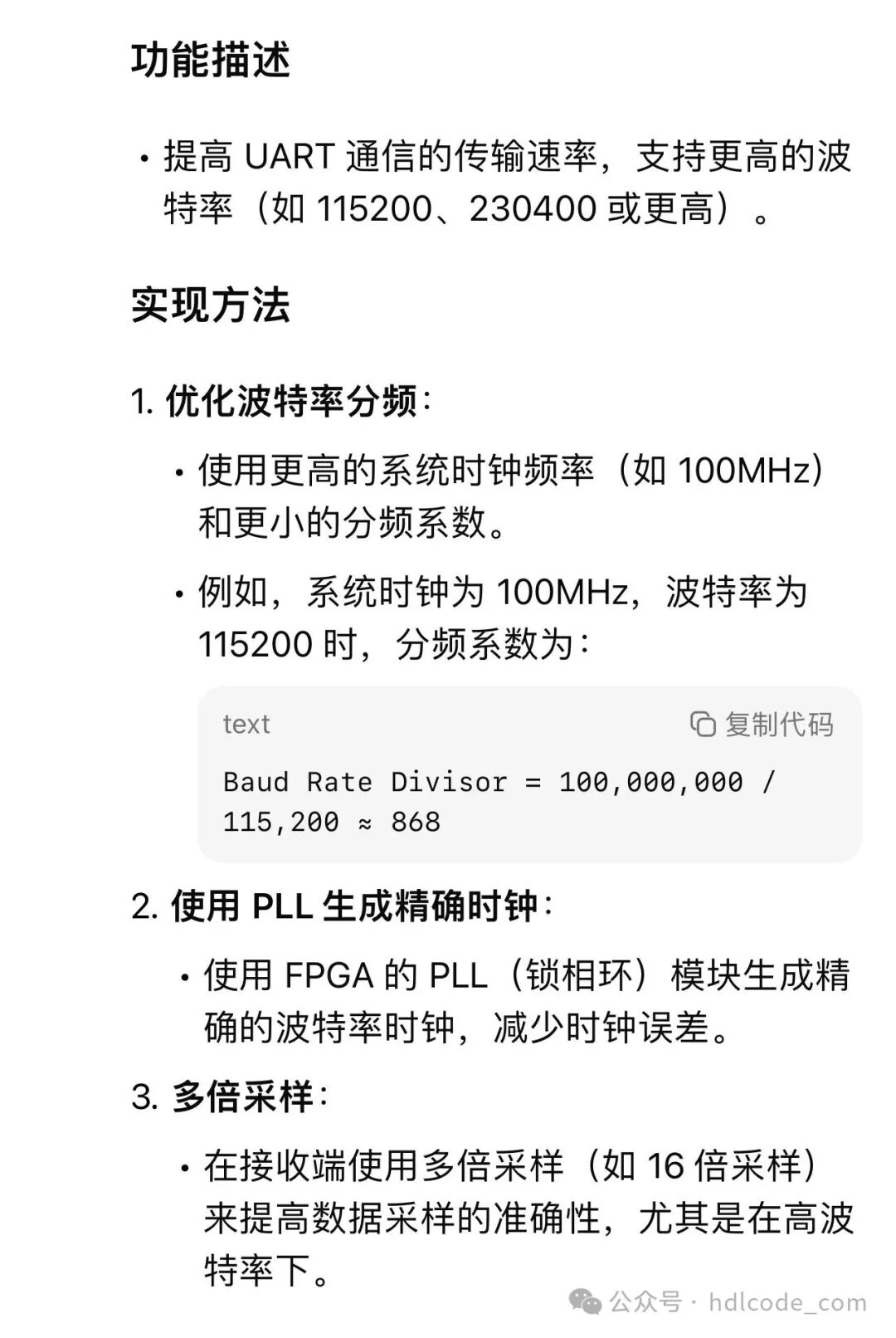
Enhance the transmission rate of UART communication, supporting higher baud rates (such as 115200, 230400, or higher).
Implementation Method
1. Optimize Baud Rate Division
Use a higher system clock frequency (e.g., 100MHz) and a smaller division factor.
For example, with a system clock of 100MHz and a baud rate of 115200, the division factor is
text 0 copy code
Baud Rate Divisor 100, 000, 000 / 115,200 ≈ 868
2. Use PLL to Generate Accurate Clock
Utilize the FPGA’s PLL (Phase-Locked Loop) module to generate an accurate baud rate clock, reducing clock errors.
3. Oversampling
Use oversampling (e.g., 16 times) at the receiver to improve data sampling accuracy, especially at high baud rates.
Editor
Editor
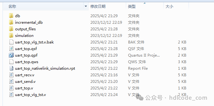
1. Project Files
Editor
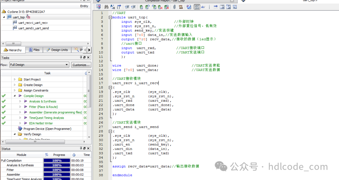
2. Program Files
Editor
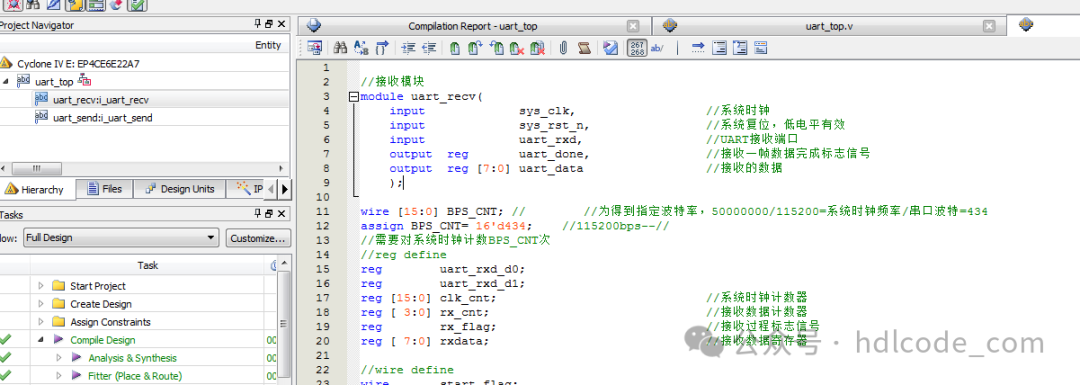
Editor
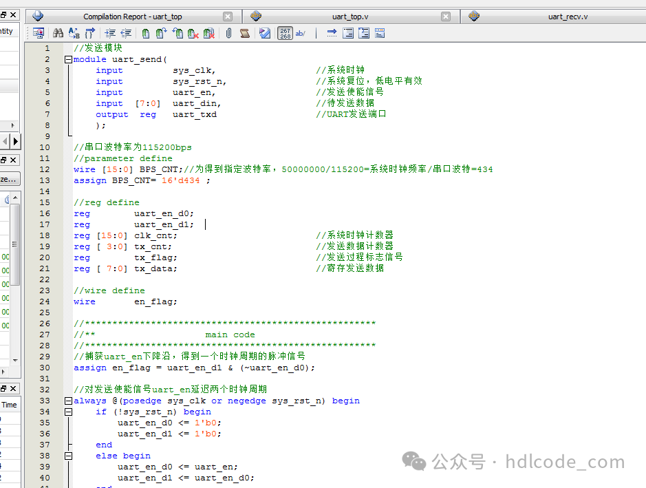
Editor
3. Program Compilation
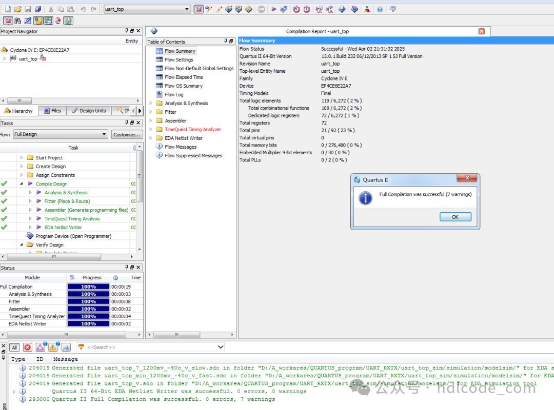
Editor
4. RTL Diagram
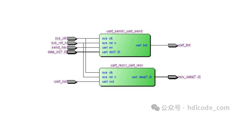
Editor
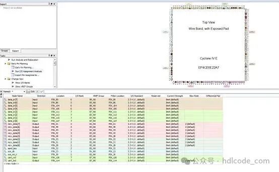
5. Pin Assignment
Editor
6. Simulation Diagram
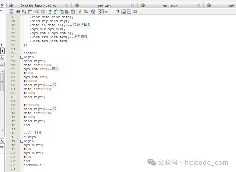
Testbench
Editor
Simulation Diagram
Top Module
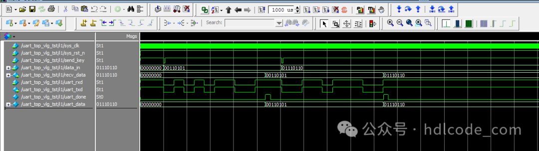
The UART baud rate is 115200. During simulation, to facilitate verification of correctness, the sending and receiving are looped back to verify if the received data equals the sent data.
Editor
The above figure shows the top module, which sequentially sent 0x35 (00110101) and 0x76 (01110110). It can be seen that the receiver successfully received these two numbers.
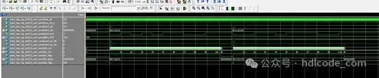
Sending Module
Editor
Waveform of sending 0x35 (00110101) and 0x76 (01110110)
Receiving Module
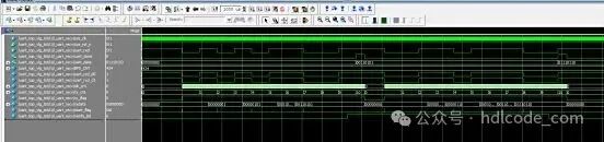
Editor
Waveform of receiving 0x35 (00110101) and 0x76 (01110110)
Partial Code Display:
// Receiving Module
module uart_recv(
    input    sys_clk,                  // System Clock
    input             sys_rst_n,                // System Reset, active low
    input             uart_rxd,                 // UART Receive Port
    output  reg       uart_done,                // Frame Data Reception Complete Flag Signal
    output  reg [7:0] uart_data                 // Received Data
);
    wire [15:0] BPS_CNT; //        // To achieve the specified baud rate, 50000000/115200 = System Clock Frequency / Serial Port Baud Rate = 434
    assign BPS_CNT = 16'd434;    // 115200bps--// // Need to count the system clock BPS_CNT times
    // Register Definitions
    reg        uart_rxd_d0;
    reg        uart_rxd_d1;
    reg [15:0] clk_cnt;                             // System Clock Counter
    reg [ 3:0] rx_cnt;                              // Received Data Counter
    reg        rx_flag;                             // Reception Process Flag Signal
    reg [ 7:0] rxdata;                              // Received Data Register

    // Wire Definitions
    wire       start_flag;

    //*****************************************************
    //**                    Main Code                    **//
    //*****************************************************

    // Capture the falling edge of the receive port (start bit), obtaining a pulse signal of one clock cycle
    assign  start_flag = uart_rxd_d1 & (~uart_rxd_d0);

    // Delay the data of the UART receive port by two clock cycles
    always @(posedge sys_clk or negedge sys_rst_n) begin
        if (!sys_rst_n) begin
            uart_rxd_d0 <= 1'b0;
            uart_rxd_d1 <= 1'b0;
        end
        else begin
            uart_rxd_d0  <= uart_rxd;
            uart_rxd_d1  <= uart_rxd_d0;
        end
    end

    // When the pulse signal start_flag arrives, enter the reception process
    always @(posedge sys_clk or negedge sys_rst_n) begin
        if (!sys_rst_n)
            rx_flag <= 1'b0;
        else begin
            if(start_flag)                          // Detect start bit
                rx_flag <= 1'b1;                    // Enter reception process, flag rx_flag goes high
            else if((rx_cnt == 4'd10) && (clk_cnt == BPS_CNT/2))
                rx_flag <= 1'b0;                    // Count to the middle of the stop bit, stop the reception process
            else
                rx_flag <= rx_flag;
        end
    end

    // After entering the reception process, start the system clock counter and the received data counter
    always @(posedge sys_clk or negedge sys_rst_n) begin
        if (!sys_rst_n) begin
            clk_cnt <= 16'd0;
            rx_cnt  <= 4'd0;
        end
        else if ( rx_flag ) begin                   // In the reception process
            if (clk_cnt < BPS_CNT - 1) begin
                clk_cnt <= clk_cnt + 1'b1;
                rx_cnt  <= rx_cnt;
            end
            else begin
                clk_cnt <= 16'd0;               // Reset the system clock counter after counting to one baud rate period
                rx_cnt  <= rx_cnt + 1'b1;       // Increment the received data counter
            end
        end
        else begin                              // End of reception process, reset counters
            clk_cnt <= 16'd0;
        end
    end