Zha Tianyi1, Chen Shengqi2, Ge Junyao3
(1. Changshu High School, Jiangsu Suzhou 215500; 2. Department of Electrical Engineering and Applied Electronic Technology, Tsinghua University, Beijing 100084;
3. School of Communication and Information Engineering, Nanjing University of Posts and Telecommunications, Jiangsu Nanjing 210023)
Abstract: This paper adopts the fractional-N phase-locked loop (PLL) chip ADF4351 as the sampling clock generator, utilizes FPGA for equal precision frequency measurement, and applies the principle of sequential equivalent sampling using the difference frequency method to design a high-speed oscilloscope equivalent sampling system with a maximum equivalent sampling rate of 160 GS/s. Meanwhile, an alternating sampling clock is generated through a clock distributor and digital delay line, and four 8-bit ADCs with a maximum sampling rate of 250 MS/s are used for time-interleaved sampling, achieving a maximum real-time sampling rate of 1 GS/s. Due to the use of a low-jitter clock source, the system maintains good noise performance within a design bandwidth of DC to 500 MHz, with a signal-to-noise ratio superior to that of equivalent sampling systems based on DDS technology.
Keywords: fractional-N phase-locked loop; equivalent sampling; time-interleaved sampling; high-speed oscilloscope
Chinese Classification Number: TN911.8; TM935.38
Literature Identification Code: A
DOI: 10.16157/j.issn.0258-7998.2017.05.023
Chinese Citation Format: Zha Tianyi, Chen Shengqi, Ge Junyao. Design of equivalent sampling system for high-speed oscilloscope based on PLL[J]. Application of Electronic Technique, 2017, 43(5): 94-97.
English Citation Format: Zha Tianyi, Chen Shengqi, Ge Junyao. Design of equivalent sampling system for high-speed oscilloscope based on PLL[J]. Application of Electronic Technique, 2017, 43(5): 94-97.
0 Introduction
In response to the application of high-speed oscilloscopes, this paper designs a difference frequency method equivalent sampling system based on fractional-N phase-locked loop technology[1], whose maximum equivalent sampling rate increases with the frequency of the measured signal, providing an inherent advantage when processing high-frequency signals. Compared with mainstream equivalent sampling schemes based on DDS (Direct Digital Synthesizer) technology, it exhibits better reliability at high frequencies. Meanwhile, this system improves the real-time sampling rate[2] through time-interleaved sampling, accommodating the performance of both periodic and non-periodic signal acquisition.
1 System Design Scheme
1.1 System Block Diagram
As shown in Figure 1, the sampling system mainly consists of peripheral circuits and digital circuits within the FPGA. During equivalent sampling, the triggering circuit and frequency division circuit first generate a square wave for frequency measurement, and after the equal precision frequency measurement module measures the signal frequency, the program built into the NIOS II soft core calculates the required sampling clock frequency and controls the phase-locked loop (PLL) module to generate the sampling clock. Subsequently, the ADC completes signal acquisition driven by the sampling clock, and the acquired data is received by the data buffer module, followed by secondary sampling in the integer sampling module and fractional sampling module, discarding excess sampling points within the same cycle as needed and correcting the equivalent sampling rate error. Finally, the sampled data is stored in RAM and sent to the oscilloscope’s human-computer interaction section.
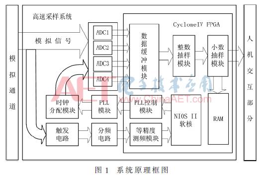
When performing time-interleaved sampling, the clock distribution module fans out the clock output from the PLL module into four paths, and uses digital delay lines to delay three of them by 1/4, 2/4, and 3/4 clock cycles, respectively, with one path remaining undelayed to form four alternating sampling clocks with phase differences of 90° each, driving four 250 MS/s 8-bit ADC chips, AD9481, to achieve an alternating sampling rate of 1 GS/s.
1.2 Theoretical Analysis of the System
1.2.1 Principle Analysis of Sequential Equivalent Sampling Using Difference Frequency Method[3]
Different phase points in a periodic signal will repeat in each cycle, so as long as each sampling point moves through ΔT in its relative position within the cycle, sequential equivalent sampling can be completed, restoring the periodic signal. When using the difference frequency method for sequential equivalent sampling, the frequency of the periodic signal f is first determined, and then a sampling clock fclk with a frequency of f/n-Δf is generated. Since the periods of the two differ by ΔT, every cycle causes the relative position of the sampling point to move through ΔT. When the last sampling point has moved through one signal cycle relative to the first sampling point, sampling of a complete cycle is accomplished.

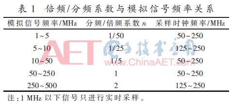
Since the analog bandwidth of this system is DC to 500 MHz, and the ADC sampling clock range is 20–250 MHz, the analog bandwidth exceeds the sampling clock range. Therefore, different multiplication/division coefficients n need to be selected based on the frequency of the analog signal (see Table 1). When n<1, the integer sampling module needs to perform secondary sampling on the sampling sequence at an n:1 ratio, discarding excess sampling points within the same cycle.
Thus, the final system’s equivalent sampling rate is:
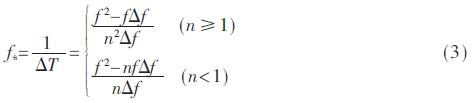 Since in this system Δf<<f, formula (3) can also be approximated as:
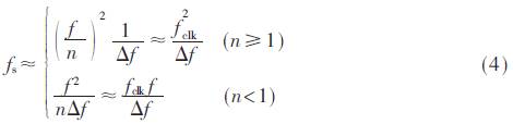 From formula (4), it can be seen that for a system with a frequency resolution of Δf, when the value of n is fixed, the maximum equivalent sampling rate of the system is proportional to f2. Therefore, this equivalent sampling method is very suitable for sampling high-frequency signals, as long as a sufficiently small Δf can be produced, a sufficiently high equivalent sampling rate can be obtained with a low-speed ADC when n is large.
1.2.2 Impact of Sampling Clock Jitter on System Vertical Accuracy
Clock jitter imposes significant limitations on the sampling accuracy of high-speed sampling systems. When the input frequency is f for a full-scale sine wave signal, the upper limit of the system’s signal-to-noise ratio due to clock jitter can be estimated by the following formula[4]:
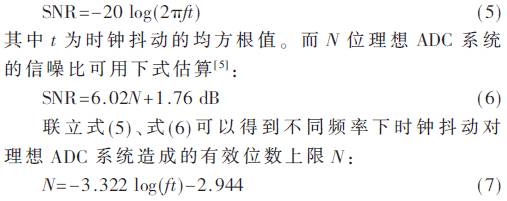
Current equivalent sampling using the difference frequency method is mostly based on DDS technology, which has poor noise performance at high frequencies. Taking the high-performance DDS device AD9854 as an example[6], its typical RMS jitter when used as a clock generator is 25 ps. Substituting this into formula (7) shows that at 500 MHz, the system’s vertical resolution will be limited to below 3.38 bits. To improve clock quality, this system uses the PLL chip ADF4351 to generate the sampling clock[7], which has a typical RMS jitter of only 0.4 ps. Calculations show that the upper limit of effective bits due to jitter is 9.34 bits, which is no longer a bottleneck for an 8-bit vertical resolution oscilloscope.
1.2.3 Analysis of System Time Base Adjustment Method
During testing, this system uses a screen with a horizontal resolution of 800 to display waveforms, dividing the horizontal direction into 10 scale grids (div), setting 28 time base levels within the range of 500 ps/div to 500 ms/div in steps of 1, 2, and 5. When displaying waveforms, each sampling point corresponds to a pixel point, allowing the relationship between the time base level t(s/div) and the equivalent sampling rate fs to be obtained as follows:

Where m is the number of scale grids, and P is the horizontal resolution of the screen.
From formula (8), it can be seen that there is a one-to-one correspondence between the time base t of the system and the equivalent sampling rate fs. When the time base level is set to the minimum of 500 ps/div, the system reaches the highest equivalent sampling rate of 160 GS/s. The equivalent sampling rate of the system is determined by the sampling clock frequency, so adjusting the system’s time base level requires correctly adjusting the frequency of the sampling clock based on the user’s selected time base level. Specifically, by combining formulas (1), (3), and (8), the formula for calculating the required sampling clock frequency based on the time base level and signal frequency can be obtained: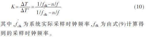
Due to the upward rounding of the FRAC parameter (see section 2.1), the actual sampling clock frequency generated by the system is always slightly higher than the calculated value, with the maximum difference being the system’s frequency step. Therefore, the fractional sampling module needs to resample the sampling data at a K:1 ratio to correct the sampling rate deviation.
2 System Software Design
2.1 ADF4351 Automatic Configuration Machine Design
Upon power-on, the automatic configuration machine first initializes the ADF4351. It sets the phase detector frequency fPFD equal to the input reference clock frequency of 10 MHz and closes the PLL loop before the output divider. At this time, the internal structure of the PLL of ADF4351 is as shown in Figure 2.
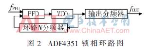
The division ratio NRF of the loop N divider is determined by three parameters: INT, FRAC, and MOD. To achieve the highest possible frequency resolution, the fractional modulus MOD is set to the maximum value of 4095. The division ratio NOUT of the output divider is determined by the range of output frequencies, as shown in Table 2.
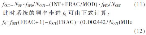
The final output frequency can be calculated by the following formula:
After initialization, the automatic configuration machine is responsible for controlling the generation of the equivalent sampling clock. Its workflow is as follows: First, based on the input signal frequency, query Table 1 to determine the multiplication/division ratio n for the sampling clock. Then, calculate the required sampling clock frequency using formula (9) and query Table 2 to determine the division ratio NOUT of the output divider; next, calculate NRF using formula (11), round NRF to obtain the value of INT, and take the integer part of the fractional part of NRF multiplied by MOD plus 1 to obtain the value of FRAC; then, write INT, FRAC, and MOD into the ADF4351 registers, allowing ADF4351 to automatically relock and update the output frequency; finally, substitute these three parameters back into formula (11) to calculate the actual sampling clock frequency, and use it to calculate the fractional sampling ratio K using formula (10).
2.2 System Software Workflow
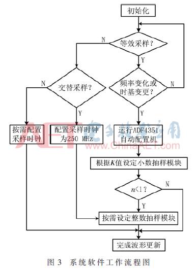
During initialization, the system performs clock skew calibration for alternating sampling. First, the front-end input is set to a 1 MHz calibration sine wave, and the sampling clock frequency is set to 250 MHz. Then, delay words of 1 ns, 2 ns, and 3 ns are written into three programmable delay lines SY89297, respectively. Finally, the delay words of the three chips are fine-tuned until the collected sine wave fits the standard waveform as closely as possible, completing the calibration. After initialization, the system waits for user input and adjusts the sampling clock in response to changes in the input signal frequency, promptly activating the ADF4351 automatic configuration machine to update the sampling clock. The system software flow is shown in Figure 3.
3 System Hardware Design
3.1 Design of Sampling Clock Source Based on Fractional-N PLL
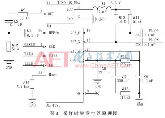
The sampling clock generator of this system is composed of the PLL chip ADF4351 and peripheral circuits, as shown in Figure 4. The reference clock source for the PLL is a crystal oscillator TCXO with a frequency of 10 MHz. The external filter loop inserted between the charge pump output CPOUT and the VCO tuning terminal Vtune is designed using ADIsim simulation software, employing a first-order passive RC filter, with a design bandwidth of 10 kHz and a phase margin of 45°.
3.2 Design of Time-Interleaved Sampling Clock Distribution Module
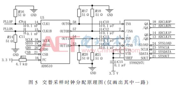
This module includes a clock distribution chip AD9510 and three digital delay line chips SY89297. The minimum delay step of this delay line is as low as 5 ps, and by fine-tuning the delay values of each clock path, clock skew caused by PCB trace delays can be effectively eliminated, reducing alternating sampling errors. However, the maximum programmable delay[8] of the chip is only 5 ns, so during alternating sampling, the sampling clock is fixed at the highest rate of 250 MHz to ensure that the clock period is less than the maximum programmable delay. Lower sampling rates are achieved through secondary sampling of the sampling sequence in the integer sampling module within the FPGA. Figure 5 shows the schematic diagram.
3.3 Design of Trigger and Frequency Division Circuit
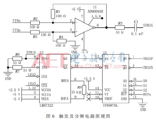
To simplify the design, the trigger signal used for frequency measurement is taken directly from the ADC input signal, which is compared with the trigger level output from the DAC after AC coupling. The resulting square wave is then divided by SY89876 and sent to the FPGA for equal precision frequency measurement. Since the ADC input signal is differential, a differential-to-single-ended converter constructed with the high-speed op-amp AD8009 is added to receive the signal and reduce the impact of the trigger circuit on the measured signal. The interface between the comparator, frequency divider, and FPGA is designed to LVDS levels to enhance transmission bandwidth and reduce slew rate, minimizing interference with the analog circuit. The output stage of the comparator’s VCCO is connected to a 2.5 V power supply to adapt to LVDS levels[9]. Figure 6 shows the circuit schematic.
4 System Performance Verification
Input a 1 MHz to 500 MHz sine wave sweep signal with a peak-to-peak amplitude of 1 V and set the time base to 500 ps/div, then read the equivalent sampling rate from the FPGA using Signal-TapII software. The measured equivalent sampling rate is always slightly above 160 GS/s within the operating bandwidth, and after adjustment by the fractional sampling module, the waveform distortion is less than 1%.
When inputting a 1 MHz sine signal with a peak-to-peak amplitude of 1 V, after enabling the time-interleaved sampling mode, the real-time sampling rate reaches 1 GS/s, with the displayed waveform distortion being less than 1%, and the second harmonic component being less than 37 dB, meeting the design requirements.
5 Conclusion
This design successfully combines equivalent sampling and time-interleaved sampling using a fractional-N PLL device to achieve a high equivalent sampling rate when processing high-frequency periodic signals.
References
[1] Zhang Junyu, Ma Xubiao. Design and Implementation of Equivalent Sampling System for Sampling Oscilloscope[D]. Chengdu: University of Electronic Science and Technology of China, 2014.
[2] Yi Min, Su Shujing, Ji Wei, et al. High-speed time-interleaved sampling system based on FPGA[J]. Application of Electronic Technique, 2015, 41(1): 71-74.
[3] Liu Ruihua, He Ming, Qiao Longfei, et al. Design of High-Speed Equivalent Sampling Oscilloscope Based on DDS Technology[J]. Laboratory Research and Exploration, 2011, 30(9): 58-62.
[4] ADI Company. Application Note: AN-501: Aperture Uncertainty and ADC System Performance[EB/OL]. (2013-11-05)[2016-11-09]. http://ec.eepw.com.cn/center/showdocument/userid/39925/id/4157.
[5] Wang Jianan, Li Zhaoji. Research and Design of High-Speed High-Precision ADC Integrated Circuit[D]. Chengdu: University of Electronic Science and Technology of China, 2008.
[6] ADI Company. AD9854 data sheet[EB/OL]. (2016-11-01)[2016-11-09]. http://www.analog.com/media/en/technical-documentation/data-sheets/AD9854.pdf.
[7] ADI Company. ADF4351 data sheet[EB/OL]. (2012-05-01)[2016-11-09]. http://www.analog.com/media/cn/technical-documentation/data-sheets/ADF4351_CN.pdf.
[8] MICROCHIP Company. SY89297U data sheet[EB/OL]. (2015-11-11)[2016-11-09]. http://ww1.microchip.com/down-loads/en/DeviceDoc/sy89297u.pdf.
[9] TI Company. LMH7322 data sheet[EB/OL]. (2013-03-01)[2016-11-09]. http://www.ti.com/cn/lit/gpn/lmh7322.