Click the above to follow us and addstar mark★ to receive timely industry news


To expand the channels for knowledge and information exchange, this journal has been included in CNKI China National Knowledge Infrastructure, Wanfang Data Knowledge Service Platform, China Core Journals (Selection) Database, and VIP Information Chinese Science and Technology Journal Database.Official submission email: [email protected]Contact: Lu Min//Abstract:Embedded component printed circuit boards are an important milestone in the transition from printed circuits to electronic circuits, transforming traditional circuit boards into true circuit boards. This article will introduce relevant knowledge.
* This article is published in “Printed Circuit Information” May 2025 (Issue No. 402)期

Author Introduction
 Gong YonglinConsultant of China Electronic Circuit Industry AssociationEditor-in-Chief of “Printed Circuit Information” Journal
Senior Engineer
00Introduction
Embedded component printed circuit boards are an important milestone in the transition from printed circuits to electronic circuits, transforming traditional circuit boards into true circuit boards. This article will introduce relevant knowledge.
01Concept and Development of Embedded Component Printed Circuit Boards
To meet the miniaturization requirements of electronic devices, the size of printed circuit boards (printed circuit board,PCB) is also trending towards miniaturization; while reducing the external dimensions of the PCB, high functionality is achieved through measures such as reducing line width and spacing and increasing the number of layers to achieve high density. However, the area for surface-mounted components on the PCB is limited to two sides, and as the surface area shrinks, it decreases, while the number of components that need to be installed continues to increase. Although the volume of components is shrinking, the limited surface area makes it increasingly difficult to meet installation requirements. Therefore, the industry often adopts new design solutions, namely, installing components within multilayer PCBs, thus forming embedded component printed circuit boards (embedded component printed circuit board,ED-PCB).
The origin of ED-PCB can be traced back to the 1970s. In low-temperature sintered ceramic multilayer PCBs, the conductive circuit patterns are formed by printing conductive ink (silver paste) on the inner layers, and then resistor ink and capacitor ink are printed on the inner circuit, forming thick film resistors and thick film capacitors. After high-temperature sintering, they become ceramic PCBs with specific circuit functions and embedded resistive and capacitive components. After the practical application of ceramic ED-PCB, it was found that ceramic PCBs have weaknesses such as high brittleness and poor processability, and they must undergo high-temperature sintering, leading to dimensional shrinkage, which affects the precision of embedded components, thus promoting the demand for the development of organic substrate materials.
There has long been a process for printing specific inks on the surface of organic substrate PCBs to form thick film resistors and thick film capacitors, and the further development requirement is to produce them in the inner layers of multilayer boards to make them embedded components. However, due to technical defects such as precision and stability, this technology has not achieved breakthroughs for a long time, until the 1980s, when Ohmega Company developed epoxy resin substrate with resistive layer material (Ohmega-Ply), and Zycon Company (later part of Sanmina-SCI) developed epoxy resin substrate with capacitive layer material (z-axis bridged capacitor,ZBC), promoting the development of ED-PCB; by the 1990s, organic substrate ED-PCB achieved mass production and application, with early typical mass application cases being Motorola mobile phones, followed by further promotion in various digital cameras and mobile phones.
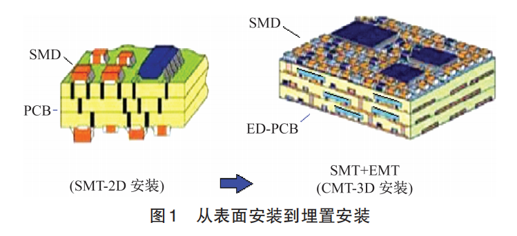
Currently, the process technology and materials of ED-PCB have been improved, and its applications are becoming increasingly widespread, such as in computers, communications, and automotive electronics. When the limited surface of the PCB cannot accommodate more components, consideration can be given to transferring them to the inner layers of the PCB, and whether it is rigid multilayer boards, flexible multilayer boards, or rigid-flex boards, components can be designed to be embedded in the inner layers. As shown in Figure 1, some surface-mounted devices (surface mount device,SMD) are transformed into embedded components (embedded device,ED), elevating surface mount technology (surface mount technology,SMT) to cubic mount technology (cubic mount technology,CMT), which is the direction of development in electronic circuit technology.
 02Characteristics of Embedded Component Printed Circuit Boards
Components installed on PCBs are usually dominated by passive components such as resistors and capacitors, accounting for over 80% of the total number of components. Therefore, ED-PCB was first developed and applied for embedding resistors and capacitors in PCBs.
In 1999, one of Motorola’s (Motorola) mobile phones had a PCB size of 40 mm×23 mm, with 89 SMDs; after adopting ED-PCB, the number of SMDs was reduced to 33, and the board size was reduced to 23 mm×23 mm. Although the cost of the PCB increased, the component and installation costs decreased, resulting in a total manufacturing cost reduction of 1 dollar per phone.
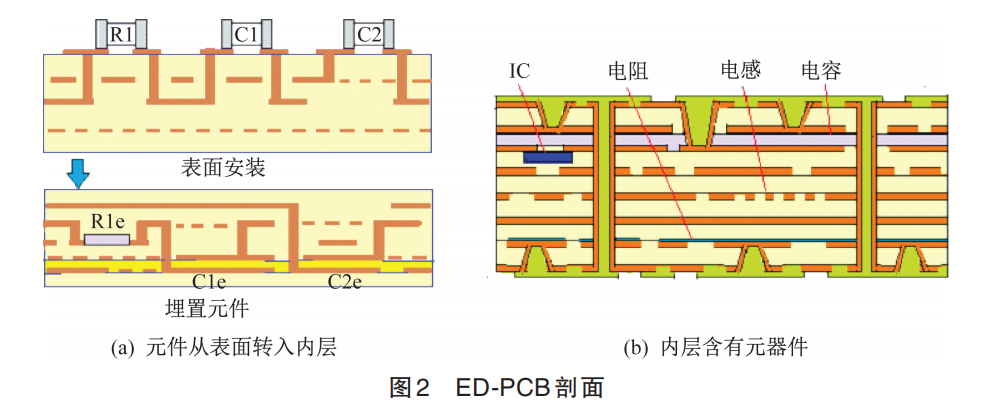
The ED-PCB technology not only promotes the installation of more components on the PCB, but also embeds components within the inner layers of the PCB, effectively reducing external solder joints, thereby improving reliability; at the same time, it can shorten the distance of connecting wires between endpoints to reduce electromagnetic interference, which is beneficial for high-frequency signal transmission.ED-PCB cross-section is shown in Figure 2, with significant advantages as follows.
(1) Increases component assembly density, reduces substrate size, and lightens weight.
(2) Increases the freedom of component layout, shortens connection lines, and is beneficial for signal transmission integrity.
(3) Reduces the number of components and solder joints during PCB assembly, improving reliability.
(4) Contributes to improving product performance and reliability while reducing overall costs.
Of course, while enhancing the functionality of the PCB, ED-PCB also increases the complexity of the PCB, making the design and manufacturing of the PCB more complex, which requires operators to continuously accumulate experience and improve technology.
……
Subsequent paper content (paid reading)↓ ↓ ↓ 3 Types of Embedded Component Printed Circuit Boards4 The Difference Between “Embedded” and “Inlaid”5 Conclusion
END
* This journal is publicly distributed domestically and internationally/monthly *Subscription methods:
1. Call 021-64139487-307 to subscribe
2. Scan the QR code below to purchase online from the PCB Knowledge Cloud Platform3. “Read the original text” to download the order
Submission Requirements
◆【Call for Papers】 The call for papers for “Printed Circuit Information” magazine has been updated, check it out quickly!
◆【Call for Papers】 Check this out! New column call for papers for “Printed Circuit Information” journal!
【Copyright All rights reserved, please contact the backend for reprint】