Click the blue text above to follow us


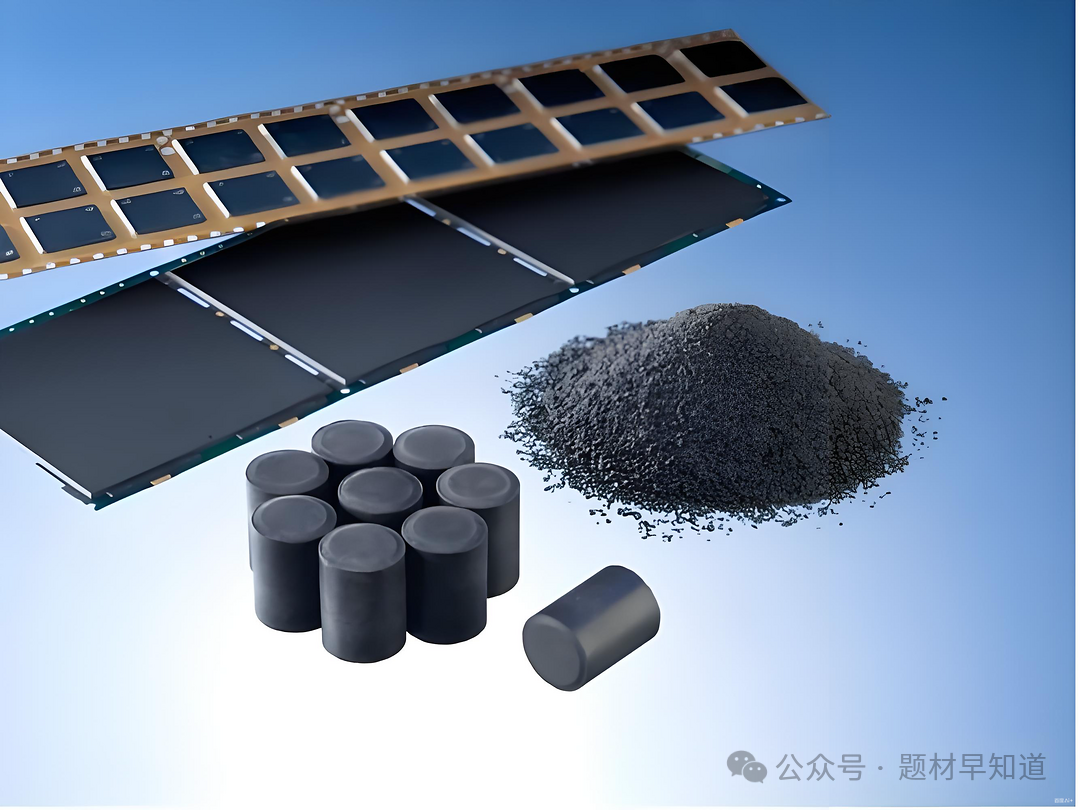
In the dim light of the chip packaging workshop, a particle with a diameter of only 0.1 millimeters is gently lifted by a vacuum nozzle, like a droplet of morning dew frozen in time. It appears ordinary, yet within the next 0.8 seconds, it undergoes 180°C melting, 0.5MPa extrusion, and a 10μm channel trek, ultimately transforming into a layer less than one-third the thickness of a human hair, isolating wafers worth hundreds of millions from external moisture, stress, and radiation forever—this “droplet” is called granular epoxy molding compound (GMC). If we compare a chip to a city of data, the silicon wafer is the foundation, and the copper interconnects are the streets, then GMC is the “quantum wall” surrounding the entire city, simultaneously fulfilling four missions of structural support, thermal management, electrical insulation, and chemical barrier within millimeters, without a single pinhole, crack, or impurity; otherwise, billions of transistors will collapse in nanoseconds due to ant holes.

Historical Overview

The first public appearance of GMC can be traced back to1976, when Sumitomo Electric in Japan used a modified toothpaste tube filling machine to inject a mixture of epoxy powder and silica into TO-92 transistor housings, solely to solve the high-temperature cracking caused by resin layering. No one expected that this “toothpaste tube experiment” would open the invisible wings of Moore’s Law: as the line width shrank from3 micrometers to3 nanometers, the chip’s tolerance to packaging stress decreased by ten thousand times, while GMC’s bending modulus increased from12GPa to28GPa, and the thermal expansion coefficient was precisely pinned at6ppm/°C—only 0.5ppm different from silicon, equivalent to controlling the thermal expansion and contraction of the Eiffel Tower to the thickness of a fingernail. Today, a 5nm mobile SoC generates a heat flux density of 120W per square centimeter at full load, exceeding that of a rocket nozzle; GMC must evenly dissipate this heat wave within 0.3 seconds while maintaining a linear shrinkage of less than 0.2% above its glass transition temperature, or the micro bumps will be torn apart, and signal integrity will distort at the femtosecond level. In other words, GMC is not a “plastic shell” but the “exoskeletal nerve” of the chip, ensuring that as electrons race through the silicon maze, they can always trust that the walls will not collapse.

“Nano City”
$
Under a scanning electron microscope, you will see that this0.1 millimeter particle is actually a “nano city”: at its core is a spherical silica coated with silane coupling agents, with a diameter of75nm, and a surface roughness of less than0.3nm, resembling a golf ball smoothed by seawater; the outer layer is an epoxy-phenolic copolymer network, with a crosslink density of up to2.4×10¹⁹cm⁻³, interspersed with precisely sized polyimide soft segments that absorb thermal stress like shock absorbers; the outermost layer is only2nm thick, a fluorocarbon layer formed by plasma polymerization, with a surface energy as low as12mJ/m², allowing the molten GMC to spread into a pore-free film on the copper lead frame rather than shrink into isolated droplets. To fit this city into a 0.1 millimeter wide mold cavity, engineers must also embed 1.2wt% of latent curing agent microcapsules within the particles, with a particle size distribution of ±5nm, ensuring it remains inert at130°C, yet completes ≥95% crosslinking within 5 seconds at180°C—like equipping each particle of dust with a timed “quantum detonator”, ensuring that the endpoint of flow is precisely the starting point of chemical bond explosion.
$

Molecular Evasion

When the packaging factory pours GMC into the mold, the real “dark matter battle” has just begun: in the10μm gap, the air between the particles must be completely expelled; otherwise, the dielectric constant of the residual bubbles is only1, while the surrounding resin is4, causing the electric field to concentrate 300% at the edges of the bubbles, enough to break down the3nm Low-k dielectric layer. To achieve this, GMC must exhibit the “shear-thinning” magic at the moment of melting—when the shear rate rises from1s⁻¹ to100s⁻¹, the viscosity drops by two orders of magnitude, like honey instantly turning into water; and when the filling is complete and shear disappears, the viscosity rises again within0.1 seconds, locking the wires in place without being displaced. This reversible “non-Newtonian dance” comes from molecular-level design: the main chain of the resin is embedded with alkyl side chains of lengths8–12 carbon atoms, which entangle with each other when at rest, but orient themselves when sheared, like trained ballet dancers instantly clearing a path, only to return to their original positions when the music ends. In experiments, we call this effect “molecular evasion”, allowing GMC to achieve100% porosity-free packaging in chip-scale packaging (CSP), with no shadows visible under X-ray, reaching aerospace-grade “zero defect” standards.

Looking to the Future
Today’s GMC has long transcended traditional packaging boundaries. At the top of the 2.5D interposer, it is laser-grooved into an array of 10μm wide trenches, then electroplated with copper, becoming a “micro-highway” between chips and silicon interlayers; in the Fan-out RDL process, GMC is compressed into 30μm thin sheets, supporting restructured wafers while maintaining warpage <50μm at 250°C, allowing lithography machines to write lines onto plastic with <50nm overlay accuracy; in quantum computing packaging, the low dielectric loss of GMC is compressed to tanδ of 0.001@10GHz, ensuring that the coherence time of superconducting qubits is not stolen by dielectric loss for 0.1 microseconds. Next-generation materials even incorporate boron nitride nanotubes into the epoxy network, targeting an in-plane thermal conductivity of 15W/m·K, ten times that of existing products, allowing 3D NAND’s 128-layer stacking to no longer be hindered by “thermal islands”.
Perhaps in the near future, when neuromorphic chips need to embed computation within the package, when optical interconnects must write polymer waveguides into the encapsulation, and when brain-machine interfaces require materials to match the elastic modulus of biological tissues, we will still return to this 0.1 millimeter particle, as if returning to the singularity of the Big Bang—small enough to drift with the wind, yet large enough to carry humanity’s ultimate imagination of computing power and connectivity. GMC teaches us: true technological revolutions often lie not in the spotlight of nanotransistors, but in the overlooked millimeter gaps; as long as there is a particle willing to dance precisely between heat and force, the epic of silicon can continue to be written, until computing power spreads across the night sky of human civilization like starlight.