Today, a customer asked us whether the programming speed of our SOP8 Flash chip would increase if the QE=1 setting is applied.
Let us revisit the concept of SPI Flash chips.
SPI FLASH typically supports the following communication modes:
Standard SPI (Single/Dual/Quad)
1. Single SPI (Single Line Mode): Uses IO0 (MOSI) to send data, IO1 (MISO) to receive data, with the clock being SCK. One transmission transfers 1 bit.
2. Dual SPI (Dual Line Mode): Uses IO0 and IO1 simultaneously, transferring 2 bits at a time.
3. Quad SPI (Quad Line Mode): Uses IO0, IO1, IO2, IO3 simultaneously, transferring 4 bits at a time, which is the fastest.
SPI FLASH pin definitions are shown in the figure below:
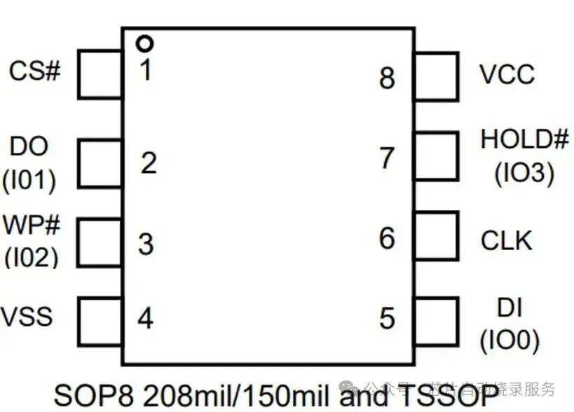
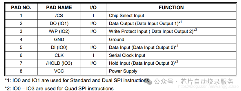
1.CS#: Chip Select, primarily used to pull low, enabling the chip under master control, indicating to the corresponding slave which one is being addressed in a parallel connection, allowing it to respond to the master‘s messages.
2.DO: DATA OUT The output pin of the chip, connected to MISO (master in slave out) when acting as a slave.
3.WP#: When the WP pin is low and software protection is not enabled, the status register does not allow writing. When software protection is enabled, WP has no effect, and writing to the status register is done through the write enable command (software protection is the default state of the chip).
4.VSS: Common ground connection GND
5.DI: DATA IN The input pin of the chip, connected to MOSI (master out slave in) when acting as a slave.
6.CLK: The clock pin, also known as SCLK/ISCK, serves as the synchronous clock signal for SPI communication, determining the communication rate and timing for reading and sending data.
7.HOLD#: HOLD When low, the DO pin becomes high impedance, and signals on DVCLK are ignored. This pin functions similarly to a pause, retaining the current state until other tasks are completed, after which HOLD is pulled high to continue previous communication.
8.VCC: The power supply range for this chip is between 1.65~3.6V, with a maximum tolerance of 0.6V.
Multiplexed Pins: Some may notice that this chip also has multiplexed pins IO0, IO1, IO2, IO3, which are used in two special modes unique to SPI FLASH. This allows the originally single DATA OUT to become IO0 and IO1 for simultaneous data transmission in Dual SPI, and IO0, IO1, IO2, IO3 for simultaneous data transmission in Quad SPI, effectively quadrupling the data throughput and temporarily converting full-duplex to half-duplex mode, enhancing data read efficiency.
1. What is the Quad Mode of SPI FLASH?
- QPI (Quad Peripheral Interface): A special four-line mode where commands are also sent via four lines, further enhancing efficiency.
2. The QE (Quad Enable) is an important configuration bit used to control whether to enable Quad Mode.
- To use Quad SPI mode (or QPI), it is usually necessary to first set the QE = 1 bit to “enable” the quad function.
2. The Role of QE (Quad Enable)
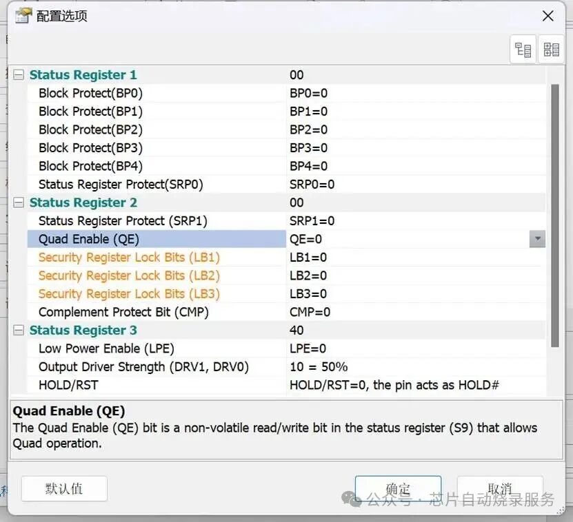
QE is a specific bit in the internal status register of SPI FLASH (Status Register), typically the 6th bit, i.e., SR2[1] or SR1[6] (the definition may vary by manufacturer), used to control whether to allow the use of Quad mode.
Specific functions include:
- Enabling Quad I/O functionality
- When QE = 1, it indicates that the use of IO2 and IO3 pins for data transmission is allowed, enabling Quad SPI mode for higher data throughput.
- When QE = 0, even if the hardware is connected to IO2 and IO3, FLASH will not use them, remaining limited to Single or Dual modes.
- Some FLASH chips that support QPI (Quad Peripheral Interface) mode also require setting QE first to switch to QPI command mode.
- For example, commands like Fast Read Quad I/O (0xEB), Quad Page Program (0x32), and Quad Input Fast Read (0x6B) all depend on QE=1 to function properly.
3. Where is the QE bit usually located?
Different manufacturers of SPI FLASH have different status register layouts, and the location of the QE bit may vary; some are in Status Register 1, while others are in Status Register-2, as shown in the figure below:
4. How to set QE?
To set QE, the following steps are generally required:
- Read the current status register (such as SR1 and SR2)
- Use Read Status Register-1 (0x05) and Read Status Register-2 (such as 0x35) to obtain the current configuration.
- Set the corresponding status register’s QE bit (for example, SR2‘s Bit 1) to 1.
- Use the Write Status Register command (which may be 0x01, 0x31, or 0x50 + 0x01, depending on the chip) to write the modified value back.
- Note: Some chips require sending the Write Enable (0x06) command first to allow modifications to the status register!
5. Why is it necessary to manually set QE?
Because: At the factory, many SPI FLASH are default disabled for Quad mode (QE = 0) for compatibility and safety. To use the high-speed Quad SPI mode (such as SPI Flash boot, high-speed downloads, QSPI Flash drivers, etc.), it is necessary to manually enable QE.
6. What happens if QE is not set?
If QE = 0 (Quad mode not enabled): Even if your hardware is connected to IO2 and IO3, FLASH will not use them. You can only use Single or Dual SPI modes, resulting in lower data transfer rates. Some commands that require Quad mode (such as 0xEB fast read) will not function properly. If your MCU or boot program (such as BootROM) is configured to use Quad SPI mode for booting, but QE is not set, it may lead to boot failure or communication errors.
Setting the QE (Quad Enable) of SPI Flash to 1 (enabling Quad mode) does not directly affect the speed of the “write program”, but if you use commands that support four lines (such as Quad Page Program), and your SPI controller is also configured for quad mode, then the write speed can significantly increase.
What factors determine the programming speed of our programmer?
The programming (Program) speed of SPI Flash mainly depends on the following factors:
1.Write command mode: Whether the write command uses Single, Dual, or Quad mode.
2.Flash programming speed: Different models of Flash have different Page Program speeds (for example, from 100µs/byte to several ms/byte).
3.Capability of the SPI controller: The master control (such as MCU, SoC) SPI or QSPI interface supports how many line modes and its clock frequency.
4.Whether Quad mode is enabled (QE=1): Only when using Quad mode write commands (such as Quad Page Program) and having Quad mode enabled (QE=1) can the four lines be utilized to enhance write speed.
5.Erase and programming process: Flash writing usually requires erasing first (Sector/Erase), which is much slower than programming, necessitating proper settings for Erase-Blank Check-Program-Verify actions.
Therefore, in summary, even if the QE=1 is set, the programming speed of the SPI Flash chip will not increase!!!
Learn the basics, understand the underlying logic, and programming is actually quite simple!!!
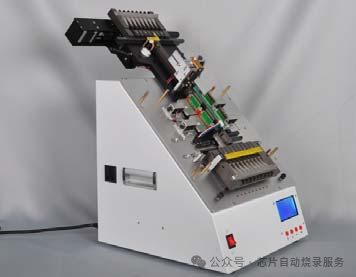
SPI Flash is the most common type in our workshop, so we support various packaging and encapsulation of chips, as shown in the figure below. We have dedicated programmers for tubular materials, for tape materials, and also automated programming equipment that supports all packaging materials.