Following the previous article, we learned about the erase, write, and read functions of FLASH, but there is still a lack of understanding regarding the relationship with JTAG. This article supplements the JTAG part.
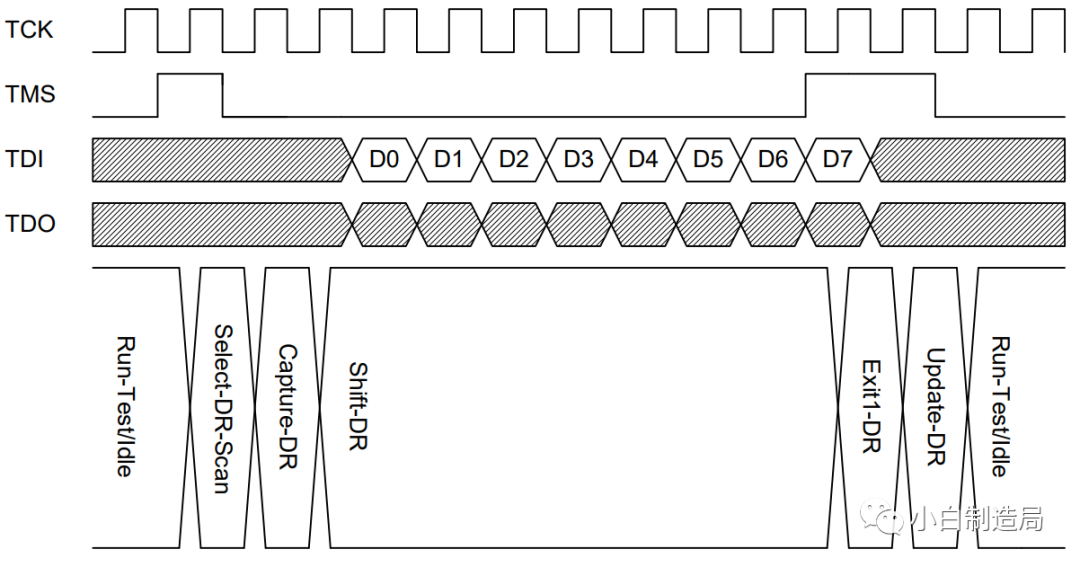
First, let’s take a look at the hierarchical structure of JTAG programming FLASH, as shown in the figure below:
The physical layer of JTAG and basic operations of the JTAG interface have already been described in previous sections; the indirect register operations, FLASH interface registers, and FLASH operations were also discussed in the last article.
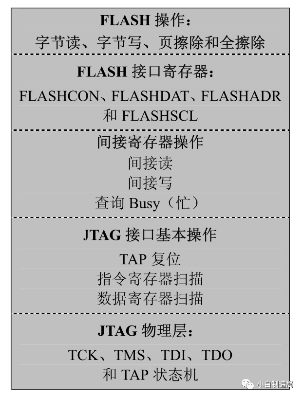
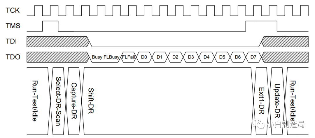
Next, by understanding the DR scan timing diagram for reading and writing FLASHDAT, we can see the role of JTAG in this process.
DR Scan Timing Diagram for Reading FLASHDAT
DR Scan Timing Diagram for Writing FLASHDAT
From the diagrams, under the clock edge of TCK, based on the TMS pattern, through the JTAG state machine including Run-Test/Idle, Update-DR, Exit1-DR, Shift-DR, Capture-DR, data writing and reading can be completed.
It is particularly important to understand that a programmer is needed for the programming process. The programmer is essentially a JTAG device, which uses a daisy chain of JTAG to write data from the programmer into the boundary scan register of the chip, and then retrieves it internally to write into FLASH.
Writing/reading data with the programmer also requires code cooperation to implement. This part requires a longer time, and we will tackle it slowly when we have time.