
Chips, as the “heart” of modern technology, have their performance iteration speed directly determining the pace of digital economy development. From the smooth operation of smartphones to the deep reasoning of artificial intelligence, from the precise control of the industrial internet to the precise calculations in aerospace, all rely on the continuous breakthroughs in chip technology. As Moore’s Law gradually approaches physical limits, the chip industry faces both the bottleneck challenges of performance improvement and the new opportunities for technological path iteration. This exploration of “breakthroughs” has long transcended the technical realm, becoming the core focus of global technological competition and industrial layout.
The Dual Path of Performance Improvement: From Device Innovation to System Integration
For a long time, the curve outlined by Moore’s Law, which states “performance doubles every 18-24 months,” has supported the rapid growth of the chip industry. The Dennard scaling law has been a key support for achieving this curve—by continuously reducing the transistor channel size, allowing more components to be integrated into a single chip, thus driving performance improvements. However, as technology nodes enter below 20 nanometers, the leakage issues of traditional planar transistors have become increasingly prominent, and the gate control over the channel approaches its limits, causing the pace of Moore’s Law to slow down. At this point, the path to improving chip performance has gradually diverged into two core paths: “bottom-up” device structure innovation and “top-down” system architecture optimization, with three cutting-edge technologies becoming the key levers for breakthroughs.
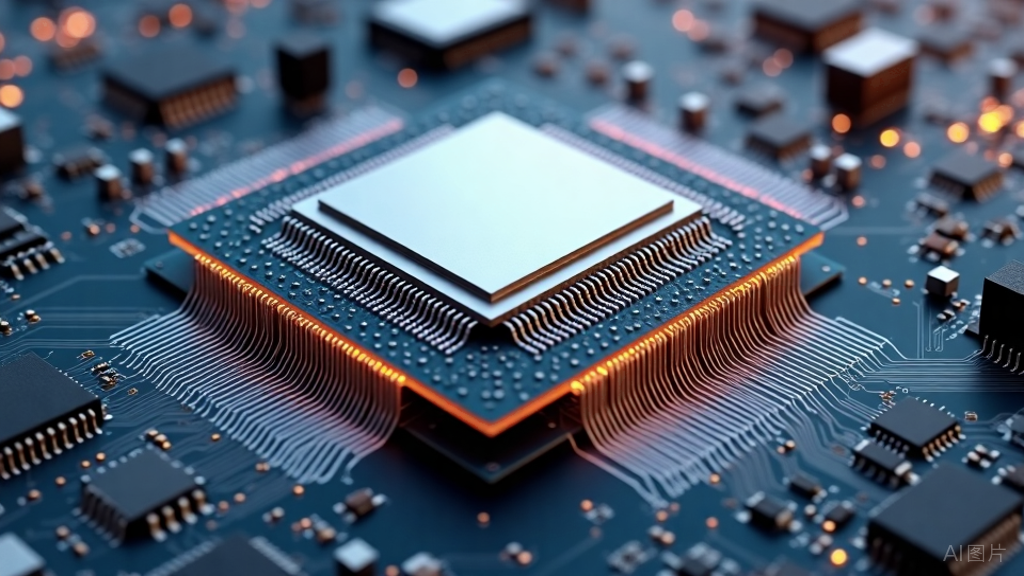
Surround-gate transistors (GAAFET) are recognized as the next-generation core devices, bearing the important mission of breakthroughs at the device level. Previously, Professor Hu Zhengming invented FinFET, which enhanced gate control through a three-dimensional structure, successfully supporting the technological implementation of 7nm and 5nm nodes. However, as nodes extend to 3nm and below, the leakage issues of FinFET have once again become a constraint. GAAFET maximizes gate control efficiency through a “gate fully wrapped around the channel” design, akin to upgrading from “covering a hillside” to “gripping a stick tightly,” completely solving the leakage risks posed by short-channel effects, making it an essential path for 3nm and more advanced process nodes. Currently, TSMC and Samsung are engaged in fierce competition in this field, and their technological breakthrough progress not only concerns their own industry positions but also affects the global high-end chip production capacity and technological direction. Moreover, the phased breakthroughs of Chinese research teams in GAAFET key technologies have laid the groundwork for breaking the overseas technological monopoly.
If GAAFET is a “single-point breakthrough,” then System on Chip (SoC) is a model of “system integration” and a core representative of the top-down path. The essence of a chip is an integrated circuit, and “increased integration” has always been the core logic of performance optimization— the more concentrated the functional modules, the shorter the signal transmission paths, leading to higher computational efficiency and lower power consumption. SoC integrates multiple functions such as CPU, GPU, memory, AI modules, and communication modules into a single chip, achieving the breakthrough of “one chip equals a complete system.” The Huawei HiSilicon Kirin 990 chip is a typical benchmark of SoC technology, integrating 10.3 billion transistors on a 7nm chip the size of a fingernail, encompassing multi-core CPU, GPU, and NPU, and being the first to achieve integrated 5G module integration. Compared to the previous generation’s separate design, it not only reduces the occupied space by nearly 50% but also enhances the collaborative efficiency of communication and computation. However, the R&D and production thresholds for SoC are extremely high, requiring the most advanced processes to meet the performance needs of all modules. The over 4,000 processes of 7nm technology, the multimillion-dollar costs of photomask plates, and the hundreds of millions of dollars in design investment make it a “technical touchstone” in the high-end chip field and an important indicator of a country’s comprehensive capabilities in chip design and manufacturing.
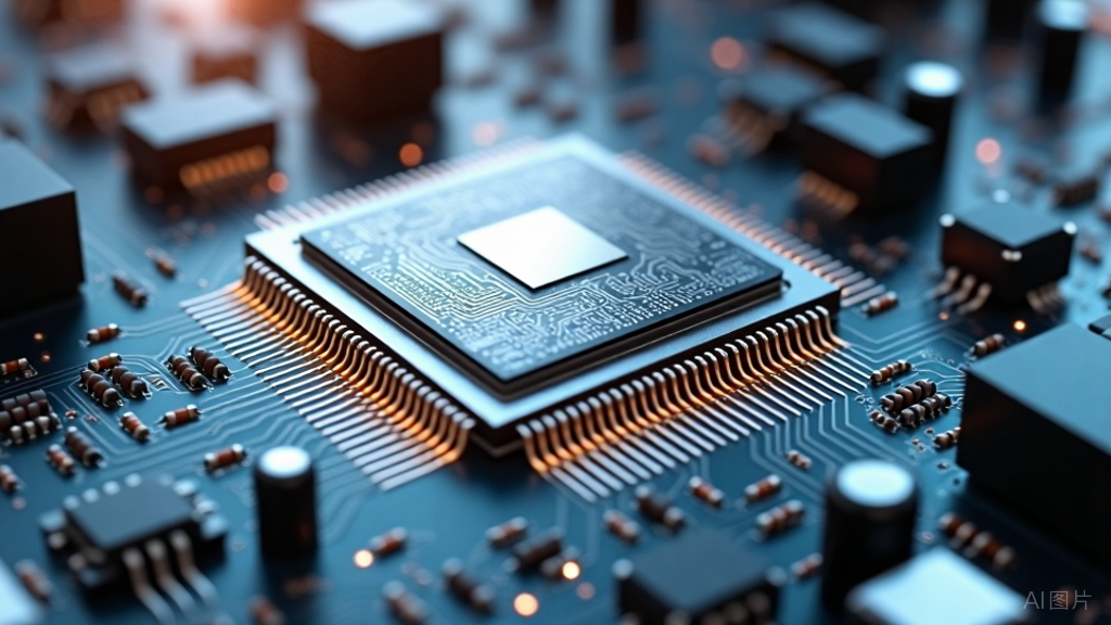
System in Package (SiP) offers another possibility for system-level optimization with its “flexible integration” approach. Constrained by the principle of a wooden barrel, SoC requires all modules to adapt to the most advanced processes, forcing modules such as storage and interfaces, which do not require high-end processes, to bear additional costs. SiP achieves efficient integration of different process modules through “multi-chip bare die co-packaging”—core modules like CPU and GPU are manufactured using advanced processes, while storage and power management modules are produced using mature processes, all integrated within the same package, preserving the integrity of system-level functions while reducing R&D difficulty and manufacturing costs. The SiP chip used in the Apple Watch achieves multiple functions in a small space through this method, balancing portability and performance needs. It is worth noting that both SoC and SiP place higher demands on EDA (Electronic Design Automation) software, requiring multi-dimensional simulations that consider electrical, mechanical, and thermal aspects. This technical challenge is not only a common challenge in the industry but also provides an important breakthrough for China’s EDA industry to break the long-standing overseas monopoly. Currently, several domestic EDA tools have achieved breakthroughs in key areas, gradually building an independent technological system.
The Controversy and Reality of Moore’s Law: Seeking New Directions at the Edge of Limits
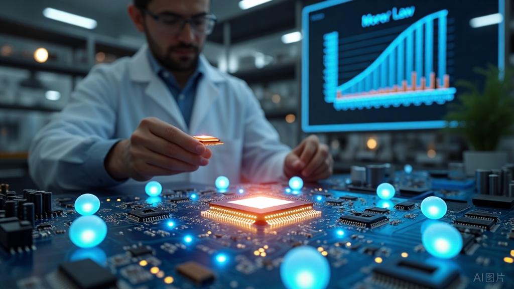
Since Gordon Moore proposed Moore’s Law in 1965, this principle has lasted for more than half a century. However, as physical limits approach, the debate over whether it has “failed” has never ceased. Silicon Valley entrepreneur Steve Blank bluntly stated that Moore’s Law has quietly failed a decade ago, with the core issue being the constraint of the “power wall”—even if transistors continue to shrink, power density remains stable. When microprocessor frequencies reached the 4GHz limit around 2005, the path of relying solely on frequency increases for performance growth has become unsustainable. The rising manufacturing costs, increasingly stringent technical barriers, and diminishing returns from performance improvements have made traditional silicon-based chip technologies face bottlenecks. Many scholars believe that the traditional logic of simply pursuing “denser components and stronger performance” can no longer support sustained industry growth.
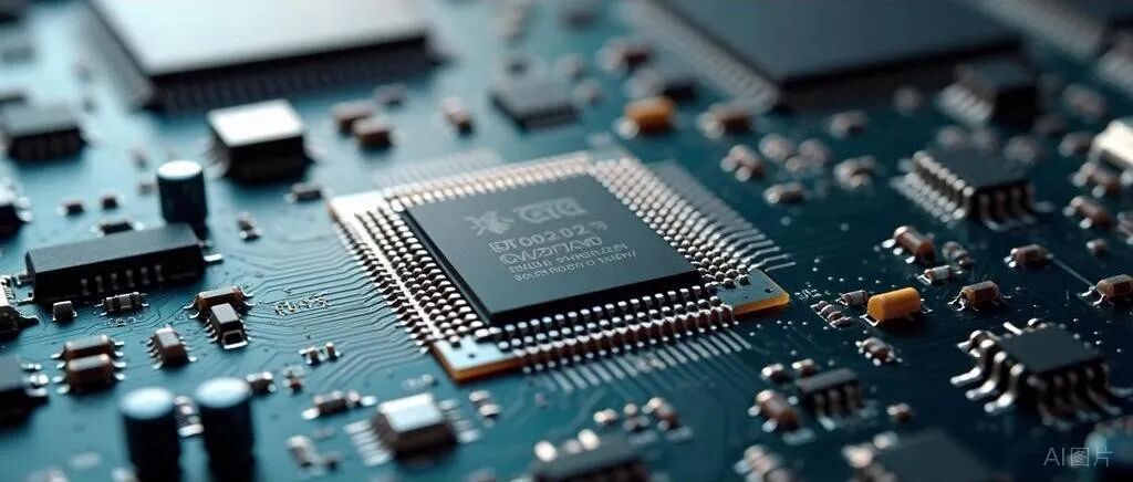
However, the controversy does not indicate a stagnation of technological innovation but rather a reconstruction of the development logic of the chip industry. Some academic viewpoints suggest that while the “doubling” logic of Moore’s Law is constrained, breakthroughs through new materials and new structures can still achieve steady performance improvements— for example, third-generation semiconductor materials such as gallium nitride and silicon carbide can achieve performance breakthroughs in high-frequency and high-power scenarios due to their higher breakdown electric fields and thermal conductivity. New technological routes such as quantum chips and photonic chips are expected to break free from the physical limitations of silicon-based materials, opening a new era of chip technology. Research data from the Institute of Microelectronics of the Chinese Academy of Sciences shows that transistors made from third-generation semiconductor materials can achieve over 30% performance improvement at the same power consumption, while quantum chips can achieve efficiencies in specific computational scenarios that are millions of times greater than traditional silicon-based chips. These explorations are providing new possibilities for the “continuation” of Moore’s Law.

More importantly, the industry has gradually shifted from “pursuing extreme performance” to “precisely matching needs.” As Blank stated, the core proposition in the current chip field has shifted from “how well can we make chips” to “what can we do with good chips.” Nowadays, in consumer electronics such as smartphones and PCs, there is a certain degree of “performance surplus,” and the perceptual differences in chip performance among ordinary users are gradually narrowing. In contrast, scenarios such as artificial intelligence, autonomous driving, and the industrial internet have precise demands for specialized chip performance— for example, AI chips focus more on parallel computing capabilities, automotive chips emphasize stability and anti-interference, while edge computing chips focus on low power consumption and real-time response. This demand differentiation means that the development of chip technology is no longer limited to the improvement of a single performance indicator but is evolving towards “customization and scenario-based” directions. The popularization of SoC and SiP technologies is a direct reflection of this evolutionary trend, achieving precise matching of chip performance and application needs through flexible combinations of functional modules.
The Global Landscape Behind Technological Competition: Chips as the Core Anchor of Technological Competition
Every breakthrough in chip technology is accompanied by a reshuffling of the global industrial landscape. As Moore’s Law approaches its limits, this competition has become even more intense, even rising to the level of national strategy. From a technological R&D perspective, the competition for technological dominance in GAAFET has become the core battleground between TSMC and Samsung. Their choices in technology routes and capacity layouts at the 3nm node directly affect the security of the global high-end chip supply chain. In the field of EDA software, overseas companies have long held over 90% of the market share, while the demand for system integration technology for multi-dimensional simulations has both raised the technical barriers and provided opportunities for Chinese EDA companies to achieve “curve overtaking.” Currently, several domestic tools have passed international certification, gradually breaking the overseas monopoly.

From an industrial layout perspective, chip technology has become a “battleground” in global technological competition. The United States is attempting to control the discourse power of high-end chip technology through the introduction of chip legislation and strengthening technology export controls, limiting the cross-border flow of advanced processes and equipment. The European Union has launched a chip plan, increasing investment in R&D and production to reduce dependence on external supply chains. China has incorporated the chip industry into the strategic emerging industries’ key layout, building an innovative ecosystem across the entire industry chain from material R&D, device design to manufacturing and packaging. The iteration of Huawei’s Kirin chips, SMIC’s breakthroughs in mature processes, and the deep cultivation of numerous startups in niche areas are gradually solidifying the foundation for the development of China’s chip industry. This global layout and competition essentially represent a struggle for future technological discourse power, and the ability to break through chip technology directly determines a country’s core competitiveness in the digital economy era.

Moore’s Law may be approaching physical limits, but the innovation in the chip industry has never ceased. From the device innovations of GAAFET to the system optimizations of SoC and SiP, from the deep exploration of silicon-based materials to the exploration of new materials, chip technology is seeking breakthrough directions along multiple paths. This battle for breakthroughs is not only about the iteration of technology itself but also about the reconstruction of the global industrial landscape and the future direction of technological civilization. In the future, the value of chip technology will no longer be measured solely by performance parameters but by its ability to precisely match diverse application scenarios and support the digital transformation of industries. In this process, the persistence of technological innovation, the construction of industrial ecosystems, and the collaboration of global resources will ultimately drive the chip industry through bottlenecks and open a new era of development.
Today’s Zen

Under the moon, the waves are calm