
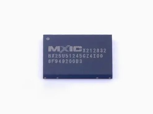
Recently, ACROVIEW, a leader in the chip programming field, launched a significant version update of its programming software. Coinciding with the release of the new version, the company announced the addition of several compatible chip models, including the MX25U51245G serial NOR flash memory developed by Macronix. This chip has successfully completed technical adaptation with ACROVIEW’s flagship AP8000 programming tool, significantly enhancing the chip compatibility and industry application range of the AP8000 series devices.
The MX25U51245G is a 512Mb serial NOR flash memory with an internal configuration of 67,108,864 x 8. When operating in dual or quad I/O mode, its structure changes to 268,435,456 bits x2 or 134,217,728 bits x4. The MX25U51245G features a serial peripheral interface and software protocol, allowing it to operate in single-line I/O mode via a simple three-wire bus. The three bus signals are clock input (SCLK), serial data input (SI), and serial data output (SO). Serial access to the device can be enabled through the CS# input.
In dual-line I/O read mode, the SI and SO pins become SIO0 and SIO1 pins, used for address/virtual bit input and data output. In quad-line I/O read mode, the SI, SO, WP#, and RESET# pins become SIO0, SIO1, SIO2, and SIO3 pins, respectively, for address/virtual bit input and data output.
The MXSMIO (Serial Multi I/O) feature of the MX25U51245G supports sequential read operations across the entire chip. After issuing programming/erasing commands, an automatic programming/erasing algorithm is executed to program/erase and verify the specified page or sector/block location. Programming commands can be executed based on byte, page (256 bytes), or word; erasing commands can be executed based on sector (4K bytes), block (32K bytes), block (64K bytes), or the entire chip.
To facilitate user interface operations, the device includes a status register to indicate chip status. By issuing a status read command, the WIP bit can be used to detect the completion status of programming or erasing operations. When the device is not in operation and CS# is high, it enters standby mode.
The MX25U51245G utilizes Macronix’s proprietary memory cell technology, ensuring reliable data retention even after 100,000 programming and erasing cycles.
Features
• Supports Serial Peripheral Interface (SPI) – Mode 0 and Mode 3
• Single power supply operation
– Read, erase, and programming operation voltage range: 1.65 to 2.0 volts
– 512Mb storage structure: 536,870,912 x 1 bit (single-line mode) or 268,435,456 x2 bits (dual-line I/O mode) or 134,217,728 x4 bits (quad-line I/O mode)
• Protocol support
– Single-line I/O, dual-line I/O, and quad-line I/O
• Latch protection: withstands 100mA current in the voltage range of -1V to Vcc+1V
• Fast read feature in SPI mode
– Supports fast clock frequencies up to 166MHz
– Supports Fast Read, 2READ, DREAD, 4READ, QREAD commands
– Supports Double Data Rate (DTR) mode
– Configurable virtual cycle count for fast read operations
• Quad-line Peripheral Interface (QPI) support
• Storage structure
– Uniform sectors (4K bytes each), uniform blocks (32K bytes each) or uniform blocks (64K bytes each)
– Any block can be individually erased
• Programming features
– 256-byte page buffer
– Quad-line input/output page programming (4PP) to enhance programming performance
• Typical erase/program cycle: 100,000 times
• Data retention time: 20 years
Software features
• Input data format
– 1-byte command code
• Advanced security features
– Block lock protection
– BP0-BP3 and T/B status bits define the size of the protected area to prevent unauthorized programming and erasing operations
– Advanced sector protection features
• Additional 8K-bit one-time programmable memory (OTP)
– Unique identifier function
– Factory lock identifiable, customer lockable
• Command reset function
• Programming/erasing pause and resume operations
• Electronic identification
– JEDEC standard: 1-byte manufacturer ID and 2-byte device ID
– RES command: read 1-byte device ID
– REMS command: read 1-byte manufacturer ID and 1-byte device ID
• Supports Serial Flash Discoverable Parameters (SFDP) mode
Hardware features
• SCLK input
– Serial clock input
• SI/SIO0
– Serial data input, or as serial data input/output in dual-line I/O read mode and quad-line I/O read mode
• SO/SIO1
– Serial data output, or as serial data input/output in dual-line I/O read mode and quad-line I/O read mode
• WP#/SIO2
– Hardware write protection, or as serial data input/output in quad-line I/O read mode
• RESET#
– Hardware reset pin
• RESET#/SIO3* or NC/SIO3*
– Hardware reset pin (as serial input/output in quad-line I/O read mode), or no connection (as serial input/output in quad-line I/O read mode)
* Depends on part number option
• Package type
– 16-pin small outline package (SOP, 300mil)
– 24-ball ball grid array package (BGA, 5×5 ball array)
– 8-pad wafer-level chip-scale package (WSON, 8x6mm, 3.4×4.3EP pads)
– All devices comply with RoHS standards and are halogen-free
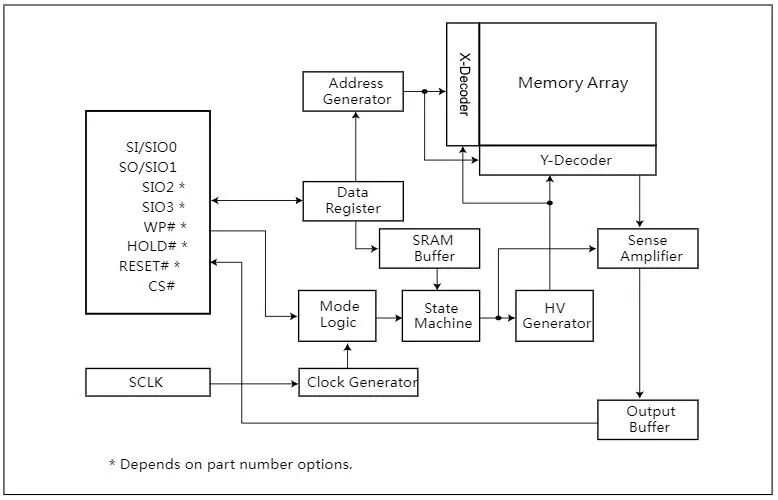
Internal Block Diagram
With a strong technical foundation, ACROVIEW’s self-developed AP8000 universal programmer is regarded as a benchmark programming solution in the industry. This device supports flexible one-to-one and one-to-eight configurations, while providing both online and offline operating modes. It has also developed dedicated programming solutions for eMMC and UFS storage chips, fully meeting the bare chip offline programming and on-board programming needs of all series of Macronix chips. The AP8000 consists of three core modules: host, baseboard, and adapter, and this modular design endows it with excellent compatibility and expandability. As a universal programming platform, the AP8000 can adapt to various programmable chips on the market and, with its stable and efficient performance, has become the core component of ACROVIEW’s automated IPS5800S programming system, efficiently handling large-scale chip programming tasks to meet mass production needs.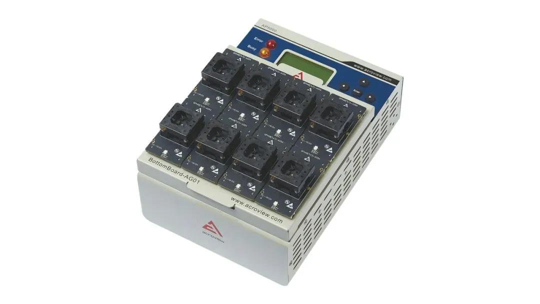
The AP8000 host features flexible connectivity options and is equipped with USB and NET interfaces, allowing for easy networking of multiple programmers. Through the networking function, users can easily achieve synchronized control of multiple programmers, efficiently conducting parallel programming operations. In terms of safety, the host is equipped with an intelligent safety protection circuit that can monitor the chip placement status and circuit connection in real-time. If it detects abnormal conditions such as chip reverse insertion or short circuits, it will immediately trigger a power-off protection mechanism, fully safeguarding the safe operation of the chip and programmer. The host is equipped with a high-speed FPGA chip, significantly enhancing data transmission and processing efficiency, ensuring a smooth and efficient programming process. To enhance user convenience, the back of the host is equipped with an SD card slot, allowing users to store project files generated with a PC onto the SD card and insert it into the slot. They can then complete file selection and loading for programming operations using the physical buttons on the programmer, achieving independent operation without a PC. This design not only reduces dependence on computer hardware configurations but also simplifies the setup process of the working environment, significantly enhancing operational flexibility.
In terms of expandability and compatibility, the AP8000 adopts a modular design of baseboard and adapter, effectively extending the functional boundaries of the host. Currently, the device has achieved support for products from all major semiconductor manufacturers, covering well-known brands such as SINOWEALTH, SemiDrive, Winbond, Holychip, and ESMT. It supports a wide range of device types, including NAND, NOR, MCU, CPLD, FPGA, EMMC, etc., and is fully compatible with various industry-standard file formats such as Intel Hex, Motorola S, Binary, and POF, providing users with a one-stop, all-scenario chip programming solution.
Company Introduction
About Macronix: Macronix is a leader in innovative non-volatile semiconductor memory solutions and the largest supplier of ROM and serial NOR Flash products in the world. Its products have been applied in consumer, communication, computer, automotive electronics, and other related fields. Macronix is one of the few companies that can provide a complete Serial Flash product range from 512Kbit to 256Mbit, and offers ultra-small Flash products that fully meet the demand for increasingly thin and compact portable electronic devices.
About ACROVIEW: ACROVIEW is a national-level specialized and innovative “little giant” enterprise engaged in the research, production, and sales of semiconductor chip testing and programming equipment. The company is committed to empowering the entire industry chain customers, including Fabless, IDM, OSAT, wafer fabs, and end-device companies, through innovative semiconductor testing technologies and solutions. ACROVIEW’s pioneering fully automated aging test ABI (Auto Burn-In) system greatly enhances the aging test efficiency of customer chips and reduces the Per DUT testing cost. It also provides customers with equipment products and solutions for all stages from PSV, CP, FT, BI, SLT, to programming. We perfectly integrate the leading advantages of product technology, system-level expertise, and a globally laid-out R&D and sales service network to create value for customers to gain a competitive edge in the market.
Scan to follow us

ACROVIEW Service Account

ACROVIEW Subscription Account