Follow our official account: Original Design Sharing by Attack Engineer.【All articles are completely free, available anytime after following】】The treasure trove of development materials for embedded engineers, providing chip information and design references.//==================================================//
Many friends have asked what steps should be followed to design a DCDC power supply chip PCB properly, and what the consequences are if the design is poor. Today, I will answer this question. First, it should be noted that PCB design is crucial for DCDC chips, with several potential risks as follows: A poor design can lead to issues.
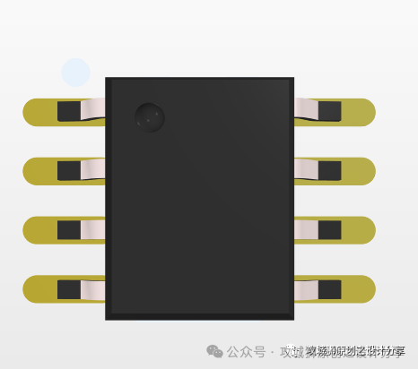
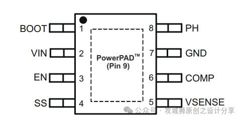
Potential Issues:
1: Poor layout of the DCDC circuit may lead to abnormal voltage readings, causing the circuit to malfunction and failing to provide accurate output voltage to the downstream load.
2: Circuit damage; many DCDC power supplies require pairing with power devices such as MOSFETs and diodes. If the PCB design is poor and heat dissipation is inadequate, these components may burn out, damaging the circuit.
3: Excessive electromagnetic radiation; this is the hardest to detect, but poor PCB design can easily lead to electromagnetic field radiation exceeding limits, failing to pass testing.
When designing DCDC chip PCB, pay attention to the following points:
1. Focus on the main circuit path in the power circuit, which is the loop where the inductor is located.
2. Pay attention to nodes where voltage changes occur in the circuit, such as SW pins.
3. Be cautious of analog signals and low-voltage digital signals that are susceptible to interference around the switching power supply to avoid disruption.
4. Minimize the routing path of voltage change circuits and shorten the feedback loop path of FB feedback.
5. Place filtering capacitors close to the pins; otherwise, their effectiveness will be reduced.
Steps for designing the PCB of a DCDC switching power supply circuit are as follows:
1. Understand the schematic and clarify the function of each component, distinguishing different loops in the circuit.
2. Place the power supply chip.
3. Place the output capacitor.
4. Place the inductor and power devices.
5. Place the input capacitor.
6. Place the analog input devices.
7. Place the digital control-related components.
8. Connect the input capacitor, inductor, and output capacitor to the output according to the current direction of the power circuit, ensuring the shortest loop, and the feedback path ground should be as close as possible to the power path, or copper should be laid under the power path to return the ground of the input pin.
9. Route the analog devices, keeping FB pins and SW pins at a distance, and keep the traces as short as possible.
10. Connect other digital signals, keeping them away from the main loop and SW pins.
11. Connect the entire copper layer below the circuit to GND, preferably as a separate GND layer, and use vias to connect the thermal pads (PAD) of the power supply chip to the copper GND to improve heat dissipation and EMC performance.
That’s all for today. Please like, follow, and share. If you have any content to add or thoughts, please leave a comment. Selected previous articles: Topology and Working Principle of Forward Converter in Switching Power Supply Reference Design for TPS54331 DCDC Buck Chip PSPICE Simulation [Lesson 4] of Transistor DC Scan Simulation