The STM32 series microcontrollers are 32-bit microcontrollers developed by STMicroelectronics based on the ARM Cortex-M series cores, including several sub-series such as F1, F4, and F7, covering various core architectures like CM0, CM3, and CM4, which can meet different selection requirements. Among them, the F1 series, as a general-purpose type, combines rich peripherals with high performance and low cost, making it the main product based on the Cortex-M3 architecture, with the most extensive applications. The F1 series includes four sub-series: F101 basic type, F102 USB-specific type, F103 enhanced type, and F105/F107 interconnect type, which only differ slightly in peripherals and memory size. The interconnect type mainly adds Ethernet support. This article mainly explains the bus architecture of the F103 series while also including some common features of other non-interconnect products in the F1 series.
STM32 Bus Architecture
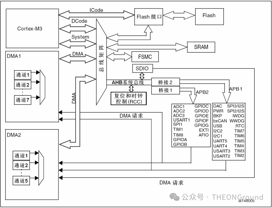 The above image shows the system structure of non-interconnect products, illustrating the main components of the chip and the bus connections between them (only the main line connections are shown in the figure). The main components include the core, memory (on-chip Flash and on-chip SRAM, etc.), peripherals, and DMA components, which are interconnected through the ICode bus (Instruction Code Bus), DCode bus (Data Code Bus), System bus, bus matrix, DMA bus, AHB bus, APB bus, and AHB2APB bridge.
Among them, the ICode, DCode, and System buses are three buses specified by the CM3 core, responsible for communication between the core and all other components. The ICode and DCode buses are also known as core private buses, which are used solely for interaction between the core and internal critical resources, achieving efficient transmission of instructions and data.
The ICode bus is a 32-bit bus based on the AHB-Lite bus protocol, responsible for reading instructions from the program memory, facilitating communication between the on-chip Flash, system memory, or external NOR Flash and the core. The ICode connects to the on-chip Flash through the Flash interface (Flash controller), which can convert the AHB-Lite protocol requests of the ICode bus into physical interface signals for Flash address latching, reading, and writing. The on-chip Flash generally stores user programs, hence also known as program memory. The system memory is a special on-chip read-only memory (ROM) pre-written and fixed with a dedicated program by ST, primarily the Bootloader, used for ISP/IAP and other boot modes, i.e., the program that runs when STM32 downloads programs via the serial port. The system memory is also connected to an internal dedicated controller (similar to the Flash controller), which is connected to the bus matrix, establishing a link with the ICode bus. For externally expanded program memory, the ICode connects to the FSMC (Flexible Static Memory Controller) through the bus matrix, while the FSMC directly connects to external expanded memory. The FSMC can convert the AHB-Lite protocol requests of the ICode bus into parallel signals for enabling read and write operations of external memory, while ensuring speed coordination between the high-speed internal bus and external memory. Typically, for STM32 series microcontrollers, the boot mode after chip reset can be determined by the high and low levels of the BOOT pin, indicating from which part the ICode starts reading the program.
The DCode bus also follows the AHB-Lite bus protocol and is an independent bus focused on data access, directly connected to the bus matrix, linking to other on-chip units (on-chip SRAM, on-chip Flash, external expanded data memory). The main access area of the DCode bus is the on-chip SRAM (storing variables, stack, intermediate computation results, etc.), and the built-in SRAM interface converts the AHB-Lite protocol requests of the DCode bus into SRAM access signals, enabling the storage and retrieval of variables in SRAM. Besides storing user programs, the on-chip Flash may also store some constants and other data, which the DCode bus accesses through the bus matrix and Flash interface. The FSMC can expand not only external program memory but also external data memory (such as SRAM), and the DCode bus can access external data memory through the FSMC.
The ICode bus and DCode bus correspond to instruction fetching and data access, respectively, reflecting the bus design of the Cortex-M3 based on the Harvard architecture, ensuring the efficient characteristic of independent access to instructions and data.The system bus does not refer to a single bus but is a bus hierarchy structure that communicates between the core and various peripherals, including the core-side System bus connecting the core to the bus matrix, the peripheral-side bus connecting various peripherals to the bus matrix, and the system module-side connections that realize communication between the core and system-level modules such as NVIC (Nested Vectored Interrupt Controller), SysTick timer, and RCC (Reset and Clock Control).
Among them, the peripheral-side bus includes two parts: the AHB system bus and the APB bus. The AHB system bus follows the AHB-Lite protocol and is the high-speed part of the system bus, connecting peripherals that require high-speed data transmission (including DMA interface, SDIO, FSMC, etc.). The APB bus is relatively slower than the AHB bus, following the APB protocol, usually connecting peripherals with lower data transfer rates. The APB bus connects to the AHB bus through the AHB2APB bridge, achieving protocol conversion between the two. STM32 has two APB buses; the APB1 bus is relatively slower, mainly connecting peripherals with lower speed requirements, while the APB2 bus is relatively faster than APB1, suitable for peripherals with certain speed requirements. For the STM32F1 series, if the AHB bus frequency is 72MHz, the maximum frequency of the APB1 bus is 36MHz, and the APB2 is 72MHz.
The bus matrix connects most of the buses on the chip and serves as a bus arbitration and routing system. It arbitrates which request to respond to first based on preset rules while managing data transmission between multiple buses, ensuring resources are transferred from the correct target address to the correct requester. The bus matrix acts like a multi-way switch, serving as a rapid response hub for information transmission between multiple buses.
The DMA bus is a dedicated bus that supports DMA data transfer, enabling data movement without CPU intervention. The STM32F1 has two DMA channel interfaces (DMA1, DMA2), and the DMA interface receives DMA requests from peripherals and initiates data transfers. The DMA bus accesses memory (SRAM, Flash, external expanded memory, etc.) through the bus matrix and connects to AHB and APB buses to access peripherals that support DMA transfers.
In summary, the STM32F1 series chip mainly consists of the core, numerous peripherals, and the connections between them. Familiarity with the core’s main operation modes, the functions of each peripheral, key registers, memory structure, and communication methods between units is essential for a deep understanding of programming the corresponding chip.