
Learn Lifelong Together, Here is Programmer Android
Recommended classic articles, through reading this article, you will gain the following knowledge points:
1. Introduction to GPIO 2. Overview of I²C Bus 3. Overview of PMIC 4. Reflection
1.Introduction to GPIO
-
GPIO: General Purpose Input Output
-
GPIOs are I/O pins that provide peripheral connections to the MSM™ chipset.
-
GPIOs can be configured as a general purpose I/O pin or alternative functions.
-
GPIOs can act as an interrupt source.
-
In a multiprocessor MSM, GPIO pins can be controlled by any master.
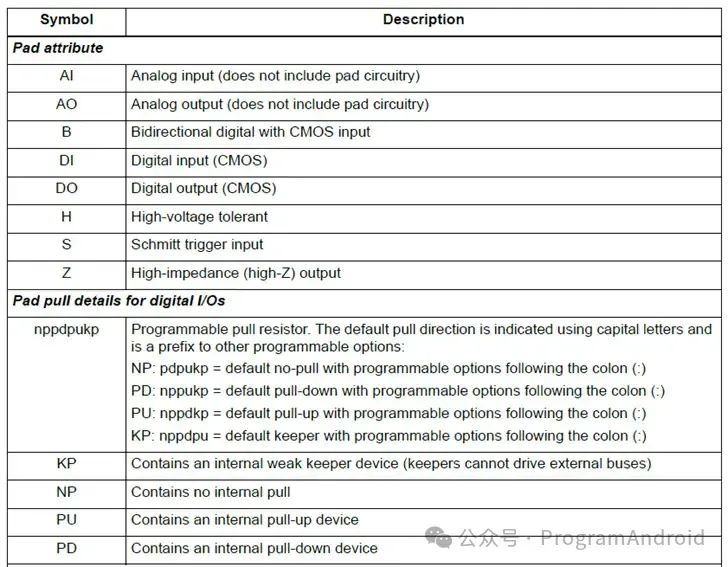
- Internal Structure of MSM GPIO
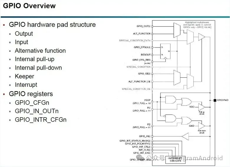
image.png
2.Overview of I²C Bus
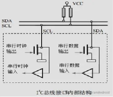
- I²C stands for Inter-Integrated Circuit, it is a two-wire interface, one Serial Data Line (SDA), and another Serial Clock (SCL).
- The internal structure is shown in the figure below:
- Speed:
- Standard mode: 100kHz;
- Fast mode: 400kHz;
- High-speed mode: 1.0MHz, 3.4MHz;
- I2C Protocol:
- The SDA transmits data in big-endian format, with each transmission being 8 bits, i.e., one byte.
- Supports multi-mastering, only one master can be present at any given time.
- Each device on the bus has its own address, consisting of 7 bits, with the broadcast address being all 0s.
- There may be multiple identical chips in the system, thus the address is divided into a fixed part and a programmable part, details depend on the chip.
- Idle State:
- The SDA and SCL signal lines of the I2C bus are both at high level during idle state, which means the bus is free. At this time, the output stage FETs of each device are in cutoff state, releasing the bus, with both signal lines pulled high by their respective pull-up resistors.
- Definitions of Start and Stop Conditions:
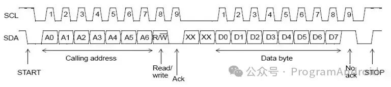
- Start Signal: When SCL is high, SDA transitions from high to low; the start signal is a level transition timing signal, not a level signal.
- Stop Signal: When SCL is high, SDA transitions from low to high; the stop signal is also a level transition timing signal, not a level signal.
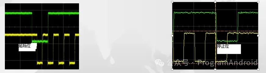
- I2C Bit Transmission
- The SDA transmits data in big-endian format, with each transmission being 8 bits, i.e., one byte.
- The address shifts left by one bit and adds the read/write bit before being sent out. Note the stop bit (master sends stop) (0: write; 1: read).
- Data Transmission: When SCL is high, if the SDA line remains stable, then data bits are being transmitted on the SDA; (data is sampled when high) if the SDA changes, it indicates the start or end of a session.
- Data Changes: The SDA line can only change the transmitted bit when SCL is low;
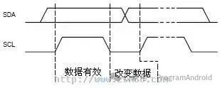
- I2C Acknowledge Signal:
- After the master sends 8 bits of data, it waits for the slave’s ACK.
- On the 9th clock, if the slave IC sends ACK, SDA will be pulled low. (Write ACK is 0, Read ACK is 1)
-
If there is no ACK, SDA will be pulled high, which will cause the master to initiate a RESTART or STOP process, as shown below:
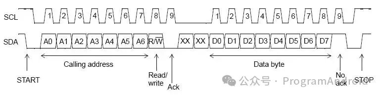
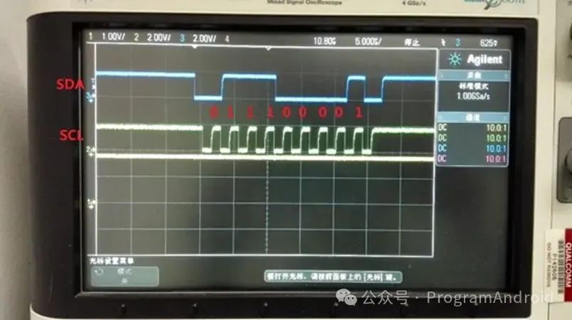
- Two Practical Examples
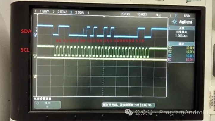
- The figure below shows the I2C waveform during failure, from the waveform it can be seen that after the host sends the I2C slave address 0x38, the slave does not respond.
- Next, let’s look at the waveform during a successful write, from the waveform it can be seen that after the I2C master sends the slave address 0x38, the slave acknowledges, the master continues to send the register address to be written 0xA5, the slave acknowledges; the master continues to send the value to be written to the register 0x03, the slave acknowledges. Communication is complete.
3.Overview of PMIC
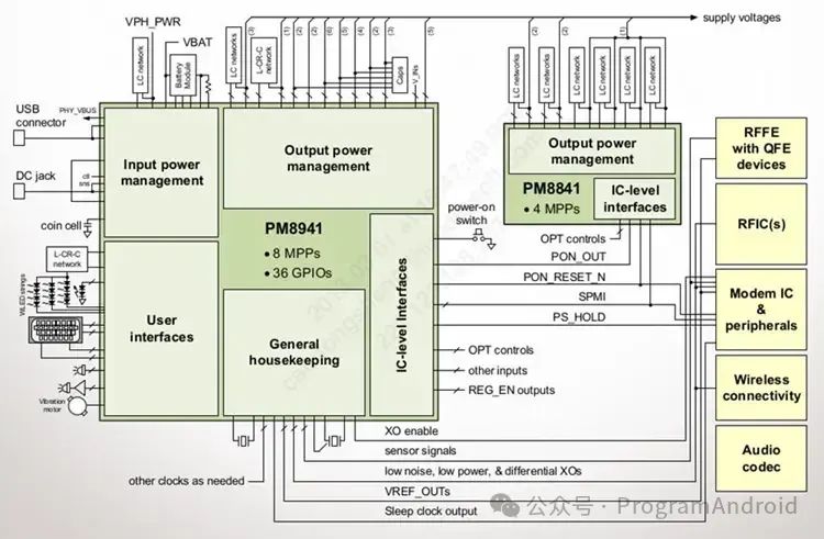
- PMIC: Power Management IC
- Includes the following main functions
- 1) Input Power Management
- 2) Output Power Management
- 3) General Housekeeping
- 4) User Interfaces
- 5) IC-level Interfaces
- 6) PMIC Configurable I/Os
- Taking PM8941 as an example, the block diagram is as follows:
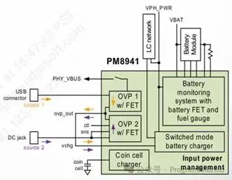
- Input Power Management:
- Dual charging and over-voltage protection (OVP)
- Fast switching charging path
- Autonomous charging
- Boost module and efficiency
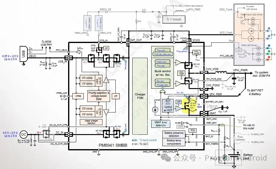
- Boost switch mode battery charger (SMBB) architecture and summary
- SMBB Architecture:
- Summary of SMBB Structure and Characteristics
- Fast automatic charging path switching with dual charging paths
- USB charging OVP is +30V, charging voltage range is 4.35~9.5V.
- DC charging path integrates +15V OVP, charging voltage range is 4.5V~9.5V, and can extend the OVP FET to achieve +30V protection
- Fully integrated high-efficiency switch-mode charger
- Charging current up to 3A.
- Switching frequency of 3.2MHz.
- Efficiency of 90% at 1A, 85% at 2.5A.
- High current voltage drop compensation.
- The boost circuit can provide 2A of current to Vchg
- Supports USB OTG, HDMI switch, LED, flash LED.
- Output Power Management Content:
- Output includes multiple buck and LDO circuits to supply different modules.
- The buck circuit is as follows:
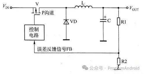
- In the figure, VIN is the input voltage, VOUT is the output voltage, L is the energy storage inductor, VD is the freewheeling diode, C is the filter capacitor, R1, R2 are the voltage divider resistors, and the feedback signal FB is generated after voltage division to stabilize the output voltage and adjust the output voltage level. The power switch V can use either an N-channel insulated gate FET (MOSFET) or a P-channel FET, and can also use NPN or PNP transistors; in practical applications, P-channel FETs are most commonly used.
- The basic working principle of a buck DC/DC converter is: the switch transistor operates in a switching state under the control of the control circuit. When the switch is on, the VIN voltage forms a loop through the switch, the energy storage inductor, and the capacitor, establishing a DC voltage across the capacitor and generating positive voltage on the left and negative voltage on the right across the energy storage inductor; during the off period of the switch, the current in the energy storage inductor cannot change instantaneously, so the inductor generates a right positive and left negative pulse voltage through self-induction. Thus, the positive voltage on the right side of the inductor to the filter capacitor and the freewheeling diode forms a discharge loop, continuing to establish a DC voltage across the capacitor, which powers the load. Therefore, the output voltage produced by the buck DC/DC converter has low ripple and low reverse peak voltage across the switch.
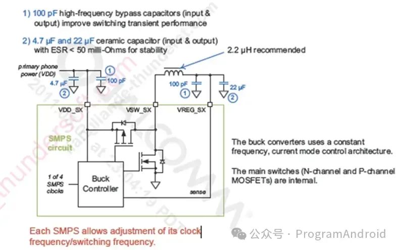
- High-throughput PMU uses synchronous rectification technology, employing dedicated power MOSFETs with very low on-resistance to replace rectifier diodes, which can reduce rectification losses and significantly improve the efficiency of DC/DC. The gate voltage of the MOSFET must be synchronized with the rectified voltage, hence the term synchronous rectification. When the output voltage drops, the forward voltage drop of the diode becomes very important, as this voltage is difficult to reduce below 0.3V, which greatly affects conversion efficiency. Using power MOSFETs with very low on-resistance results in much smaller voltage drop losses than diodes, greatly improving conversion efficiency.
- Internal Structure of High-throughput BUCK Circuit
- LDO is a low dropout regulator, which is a type of linear voltage regulator that operates at a lower voltage drop than traditional linear voltage regulators. Traditional linear voltage regulators, such as the 78xx series, require the input voltage to be at least 2V~3V higher than the output voltage to operate correctly. However, in some cases, this condition is too strict, such as when converting 5V to 3.3V, where the input-output voltage difference is only 1.7V, clearly not meeting the requirement. This is why LDO power conversion chips were developed. They have advantages such as low cost, low noise, low static current, and fewer required external components. The disadvantage is lower efficiency. The input current of an LDO is essentially equal to the output current, and the efficiency is equal to output voltage/input voltage; if the voltage drop is too large, losses will be significant.
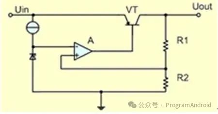
- The basic circuit of an LDO is as follows: this circuit consists of a series pass transistor, sampling resistors, and a comparator amplifier. The sampled voltage is applied to the non-inverting input of the comparator, compared with the reference voltage at the inverting input. The difference is amplified by the comparator, controlling the voltage drop of the series pass transistor to stabilize the output voltage. When the output voltage drops, the difference between the reference voltage and the sampled voltage increases, causing the comparator’s output to increase the drive current to the series pass transistor, reducing its voltage drop and thus increasing the output voltage. Conversely, if the output voltage exceeds the set value, the comparator’s output drive current decreases, causing the output voltage to drop.
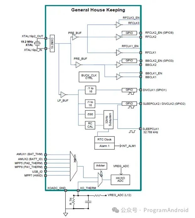
- General Housekeeping:
- HK/XO ADC circuits are shown in the figure below:
- Includes system clock and ADC
- User Interface
- Light pulse generators (LPG)
- RGB LED driver
- Flash driver
- White LED support
- Keypad interface
- Vibration motor driver
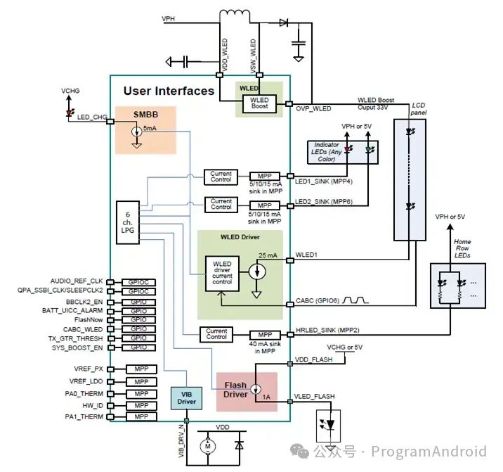
- IC-level Interfaces:
- OPT hardware configuration controls
- Programmable boot sequence (PBS)
- Power on/power off sequence
- Reset
- Under-voltage lockout
- Sudden momentary power loss (SMPL)
- SPMI and interrupt managers
- Modem power management support
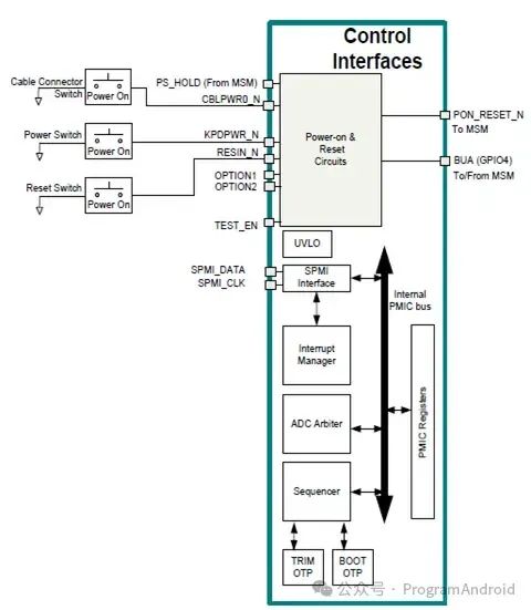
- PMIC Configurable I/Os
- GPIO
- MPP
4.Reflection
1. What modes can Qualcomm’s processor GPIO be set to?2. When does the I2C start signal occur?3. How many bits does it take to fully transmit one byte in I2C?4. What is the main function of PMIC?5. Please explain the advantages and disadvantages of BUCK and LDO.
Source: Imaging Technology StackArticle Author: AbaloneArticle Link:
https://camerastacker.com/2022/071028925.html
This article has come to an end. The editor believes that the articles shared online are excellent, welcome to click to read the original text, support the original author, if there is any infringement, please contact the editor to delete, your suggestions and corrections are welcome. We look forward to your attention, thank you for reading, thank you!

Click to see, give a thumbs up to the big guy!