There are many power reduction methods that have been in use for some time, and these are mature technologies. This chapter describes some methods for low power design.
Clock Gating
A significant portion of the dynamic power consumption in a chip is wasted in clock balancing. More than 50% of dynamic power can be wasted in clock buffers, as these buffers have the highest toggle rates in the system, there are many clock buffers, and they typically have high drive strength to minimize clock delay. Additionally, even when the input and output signals remain unchanged, the flip-flops receiving the clock dissipate some dynamic power.
The most common method to reduce this power consumption is to turn off the clocks when they are not needed. This method is known as clock gating. Modern EDA design tools support automatic insertion of clock gating: they can identify circuits, and the insertion of clock gating can be done without altering the logical functionality, as shown in Figure 2-1.
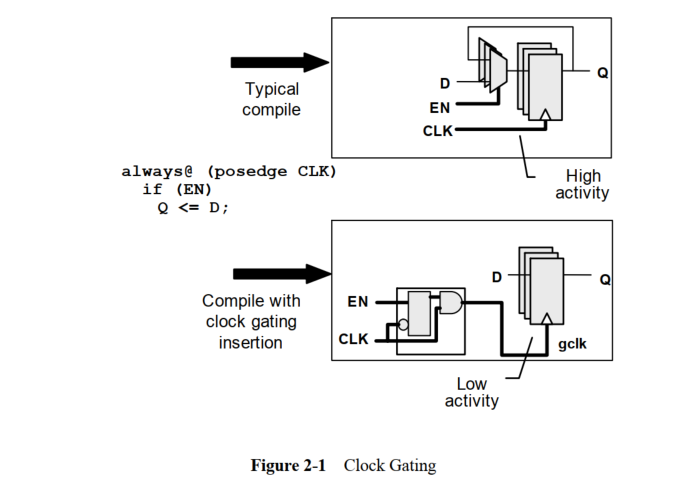
In the original RTL, whether the registers are updated depends on the variable EN. The same result can be achieved based on clock gating of the same variable.
If the involved registers are single-bit, the power savings may not be significant. If they are 32-bit registers, then a clock gating unit can control 32 registers (as well as any buffers in their clock tree). This can lead to substantial power savings.
In early RTL designs, engineers would explicitly code clock gating circuits in RTL. This method is prone to errors—it is easy to create a clock gating circuit that generates glitches, leading to functional errors. Today, most libraries, including specific clock gating cells, can be recognized by synthesis tools. Explicit clock gating libraries can be automatically inserted, making clock gating a simple and reliable method for reducing power consumption. This clock gating strategy can be implemented without any changes to the RTL.
A paper reported a unique opportunity where a team recently had to compare a (nearly) identical chip implementation with and without clock gating. As an energy-saving engineering effort, an existing circuit chip without clock gating was redesigned and implemented in a 180nm process, with only minor changes to the logic (some small blocks were removed and replaced with others).
The report showed a 20% reduction in area and a power savings of 34% to 43%. The specific power savings ratio from clock gating depends on the operating mode. The power measurements came from actual silicon, and the area savings were due to a single clock gating cell replacing multiple multiplexers.
After some analysis and experimentation, the team concluded that clock gating should only be used on signals with a bit width of at least 3 bits. Using it on 1-bit registers does not achieve a balance between area and power optimization. Most of the energy savings are due to clock gating cells being placed early in the clock path. About 60% of the clock buffers appear after the clock gating, so their activity is reduced to zero during gating.
Gate-Level Power Optimization
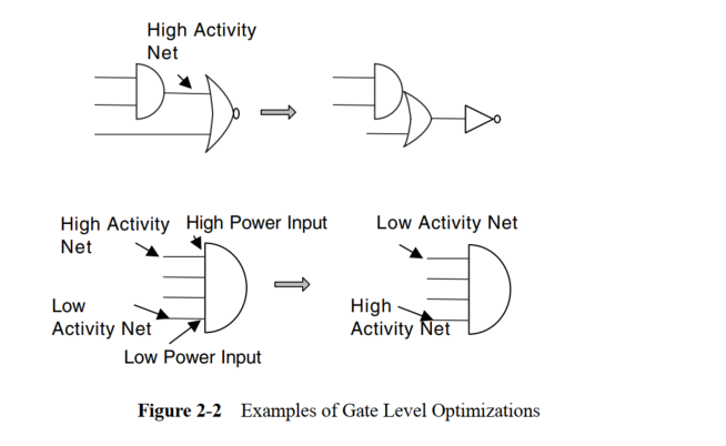
In addition to clock gating, tools can also perform some logic optimizations to minimize dynamic power consumption. Figure 2-2 shows two of these optimizations. In the upper half of the figure, the output of a gate has particularly high activity. Since it is followed by a NOR gate, these two gates can be remapped to an AND-OR gate plus an inverter, so that the high-activity network exists within the module. Now, the high-activity node (the output of the gate) drives smaller capacitance, reducing dynamic power consumption.
In the lower half of the figure, the gate has been preliminarily mapped so that a high-activity signal is connected to a high-power input pin, while a low-activity signal is mapped to a low-power pin. For multi-input gates, there can be significant differences in input capacitance and power across different pins. By remapping inputs to connect high-activity signals to low-power inputs, optimization tools can reduce dynamic power consumption.
Other examples of gate-level power optimization include changing cell sizes and buffer insertion. Regarding cell sizes, the tool can selectively increase and decrease cell drive strength across the critical path to meet timing requirements, thereby reducing dynamic power to a smaller value. In buffer insertion, the tool can insert buffers instead of increasing the drive strength of the devices themselves. If done appropriately, this can reduce power consumption. Like clock gating, gate-level power optimization is performed by synthesis and other EDA tools and is transparent to RTL designers.