 Source: Content fromhttp://www.cnblogs.com/IClearner/ , Author: IC_learner, Thank you.
This section mainly introduces the use of gated clocks for low-power design.
(4) Gated Clock
The gated clock was briefly described in my first blog; here I will provide a more detailed description. We will mainly learn what gated clock circuits are, when to use gated clocks, how to synthesize gated clocks in libraries, how to use gated clocks, some processing for gated clocks, and how to manually insert gated clocks. We will focus on how to use gated clocks and their processing.
① Overview of Gated Clocks
There are two approaches for gated clocks: one is to gate the clock directly for registers, and the other is to gate the clock at the module level. Compared to the latter, gating the clock directly for registers is more flexible. This is because, in many cases, we cannot guarantee that the registers that do not need gating are allocated in different modules from those that do. Therefore, we mainly introduce register-level gated clocks.
The following diagram shows a simple circuit of a gated clock:
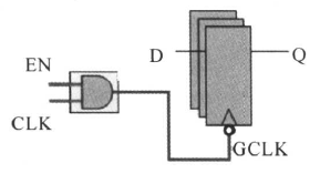
In the above circuit diagram, the control signal (EN) is directly ANDed with the clock signal (CLK) to complete the gating. The gated clock signal GCLK is sent to the register array. Thus, when EN is 0, this clock is turned off. The corresponding waveform is shown below:
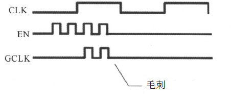
It can be seen that if the EN signal is not controlled, it will cause glitches in the gated clock signal. Glitches on the clock signal are very dangerous. Therefore, to prevent glitches in the gated clock, the enable signal must meet the following condition: it must be the output of a register, and the clock signal of that register must be the same as the clock signal to be gated. For the above reasons, although this gating method is the most direct, it is rarely used in practice.
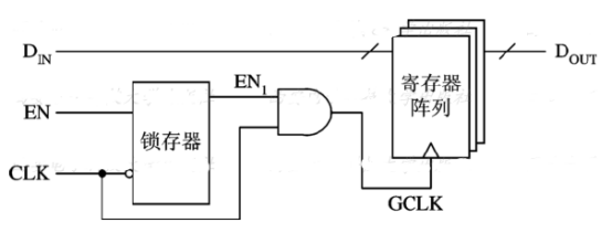
To solve this problem, a latch-based gated clock solution is introduced, as shown in the following diagram:
The corresponding timing diagram is shown below:
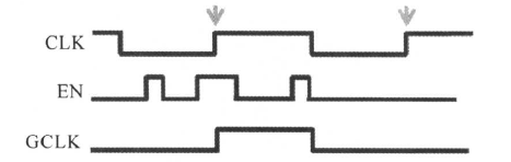
It can be seen that this method eliminates the glitches caused by the combination of EN and CLK on the gated clock. The principle of this method is that the latch is transparent when CLK is low. Thus, glitches on the EN signal only appear at the low level of CLK, and the AND operation between EN1 and CLK can eliminate these glitches. As a result, there are no glitches on GCLK.
However, it is important to note that if the latch is far from the AND gate, and the clock arriving at the latch has a significant delay difference from the clock arriving at the AND gate, glitches will still occur. The following analysis will explain this:
In the upper right diagram, the clock at point B arrives later than the clock at point A, and Skew > delay, which causes glitches. To eliminate glitches, we need to control Clock Skew to satisfy Skew > Latch delay (the delay from clk to q of the latch). In the lower right diagram, the clock at point B arrives earlier than the clock at point A, and |Skew| > ENsetup (D->Q), which also causes glitches. To eliminate glitches, we need to control Clock Skew to satisfy |Skew| < ENsetup (D->Q).
Commonly, the first type of glitch occurs, but we can make this logic into a unit, which can basically eliminate the above two types of glitches, that is:
Under normal circumstances, the clock tree consists of a large number of buffers and inverters, and the clock signal is the signal with the highest toggle rate in the design. The power consumption of the clock tree can account for up to 30% of the total design power consumption. After adding the gated clock circuit, the switching behavior of the clock tree is reduced, thereby saving switching power. Additionally, due to the reduced switching behavior of the clock pins, the internal power consumption of the registers is also reduced. Using gated clocks can effectively reduce the power consumption of the design, generally saving 20% to 60% of power consumption.
Moreover, since gated clocks do not require MUX units, the area of the design is also reduced after adding gated clock circuits. The larger the fanout of the gated clock circuit, the better the efficiency of reducing power consumption and area. Of course, if the fanout is too large, it will cause timing issues.
Gated clock circuits are very easy to implement; tools can automatically insert gated clocks without modifying RTL code, and gated clocks are independent of the process.
These advantages should have been mentioned in the summary section, but I have introduced them here to give everyone an impression. The low-power advantage is discussed throughout the article, and we will discuss the issues of reducing area and implementation in the specific implementations to follow.
② Gated Clock Models in the Synthesis Library
As mentioned earlier, gated clocks can be implemented in three ways: one with an AND gate (i.e., gated clock without latches), distributed latches + AND gates, and integrated latches + AND gates. In the synthesis library, AND gates and latches are basic logic units, so they can form gated clocks. In addition, the synthesis library also provides integrated gated cells specifically. Generally, we use integrated gated cells because they control Skew and do not have the glitch problems described earlier.
An example of a gated clock cell description in the synthesis library is shown below:
(In this synthesis library model, E is the gating signal; CK is the clock signal; ENL is the latch output; ECK is the clock signal after gating; the state table describes the function of the internal latch in this gated cell. The other contents of the unit are not described in detail; I have introduced the synthesis library in my blog under the category of Tcl and Design Compiler.)
③ Implementation of Gated Clocks
To implement gated clocks, we first need to set them in the RTL code. In the RTL code, the registers that need gating should be written in the “load-enable” form, as shown below:
always @(posedge CLK)
if (EN)
Q <= D;
In the above code, if EN is valid, the register samples the data on the rising edge of the clock; otherwise, it retains the original value. Generally, the synthesis will yield the circuit shown in the upper right corner of the diagram, while the circuit with inserted gated clocks will be as shown in the lower right corner:
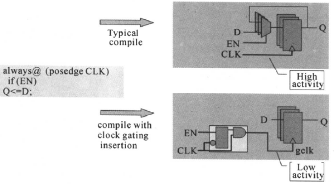
In the typical synthesis result shown in the above diagram (i.e., without using gated clocks), a MUX is added before each register controlled by the EN signal; when the EN signal is valid, the register latches the input signal D; otherwise, it retains the original value. This method can also reduce the toggling on the registers, thus saving toggle power. However, in this “load-enable” structure, each register has a MUX; assuming the area of the MUX is 4, the area required for an 8-bit register increases by 32. A larger area means higher chip costs and increased overall power consumption. Additionally, this method cannot eliminate the power consumption on the clock tree.
For the gated clock synthesis circuit shown in the lower right corner, if the area of a gating logic is 10 and a gated clock signal can drive an 8-bit register, then for every 8 registers, one gating logic is needed, resulting in an additional area of 10. Thus, we can see that the gated clock circuit has a smaller area and lower power consumption than the normal synthesis result.
Given the advantages of gated clocks, we need to convert the normal synthesis results into gated clock results, mainly achieved through the DC power compiler. We primarily use commands to set the style of gated clocks and to “enable” the insertion of gated clocks. The synthesis tool inserts the corresponding gating logic based on the clock gating style we set. Therefore, the implementation of gated clocks mainly involves two steps: one is to set the style of gated clocks using the command set_clock_gating_style and its options; the other is to add gated clocks in the netlist using the command insert_clock_gating. Below, we will introduce these two settings; since the commands differ in different versions of DC, the specific options may vary, so here we only introduce some common or potentially useful options.
Before executing the insert_clock_gating command, we generally use the set_clock_gating_style command to specify the structure of the gated clock circuit to be inserted (or the style of the gated clock to be inserted). Below, we will introduce the gated clock circuit structures that can be inserted using this set_clock_gating_style command.
-sequential_cell option sets whether to use a latch-based style. Since our gated clocks come in three forms (AND gate without latches, latch-based + discrete AND gate, integrated latch + AND gate), we need to specify which form to use:
A: The latch-based discrete gating cell is the default value, which can be set by the command below:
set_clock_gating_style -sequential_cell latch
B: The gating cell without latches can be set by the command below:
set_clock_gating_style -sequential_cell none
C: Using the integrated gating cell does not require using the -sequential_cell option because this option determines whether to use a latch-based style. To set the integrated gating cell, we can directly set the parameters, for example, we can use the command below:
set_clock_gating_style “integrated”
It is generally recommended to use the integrated gating method.
-positive_edge_logic option (abbreviated as -positive or -pos) sets the gating logic for registers triggered on the rising edge in the RTL code (i.e., registers triggered on the rising edge).
-negative_edge_logic option (abbreviated as -negative or -neg) sets the gating logic for registers triggered on the falling edge in the RTL code (i.e., registers triggered on the falling edge).
For example, the command below:
set_clock_gating_style -sequential_cell none -pos “or”
This command sets a style without latches, and for registers triggered on the rising edge, the gating unit uses OR gate logic.
set_clock_gating_style -neg “integrated”
This command sets the integrated gating clock unit for registers triggered on the falling edge in the RTL code.
set_clock_gating_style -positive “integrated” -negative “integrated”
This command sets the clock unit controlling the registers in the RTL code to use the integrated gating clock unit, regardless of whether the registers are triggered on the rising edge or falling edge.
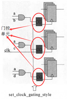
-minimum_bitwidth option is used to set the minimum width of the register array for clock gating. For register arrays with a width smaller than this setting, clock gating is not performed; however, when the circuit has a common enable signal, it will decompose the circuit for collective gating. For example, the command below has the following effect:
set_clock_gating_style -minimum_bitwidth 4
The above command means that a gated clock must trigger at least 4 registers. In the left diagram, there are three groups of registers, each with only 3 registers, which do not meet the requirement of at least 4 registers. Therefore, for each group of registers, gated clocks cannot be used. However, all three groups of registers have a common enable signal “a”, which can be decomposed and used as the gating signal for the clock. Thus, signal “a” controls 9 registers, satisfying the requirement of triggering at least 4 registers. Consequently, when the above command constrains the circuit on the left, the synthesis result will become the circuit on the right with gated clocks.
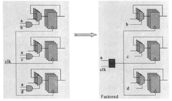
-num_stages option is used to set the number of stages for a multi-stage gated clock. In some designs, the top-level gating signal may be decomposed into different sub-gating signals. By default, only the gating signals connected to the register array generate gating logic. For example, in the following circuit diagram:
In this example, the global gating signal EN is combined with signals a, b, c, and drives different register arrays. By default (the default setting for the set_clock_gating_style command is “num_stages” equals “1”, and the default is also 1), the gating signals connected to the register arrays are provided by the gating unit.
Since all three groups of registers have a common enable signal “a”, it can be decomposed to produce an additional (stage) gated clock unit. By adding the option “-num_stages 2” to the set_clock_gating_style command, a two-stage gated clock as shown in the diagram below can be produced:
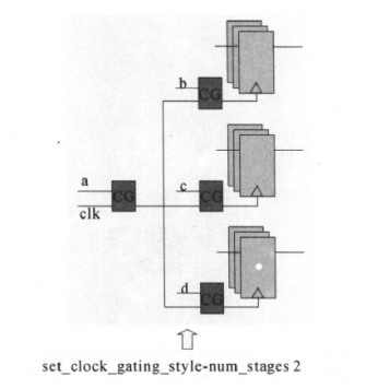
Using multi-stage gated clocks, the clock synthesizer can place the gated clock units as close to the clock source as possible, thus minimizing the power consumption of the clock tree.
-control_point and -control_signal options relate to DFT and are used to set whether the gating unit is controllable in DFT, whether the DFT control signal is scan-enable or test-mode, and whether the DFT control signal and the EN signal are combined before or after the latch in the gating logic. Typically, the DFT control signal is combined with the EN signal using OR logic, allowing control of the gating logic during DFT. For example, the command constraint below:
set_clock_gating_style -control_point before -control_signal test_mode
Sets the following circuit structure:
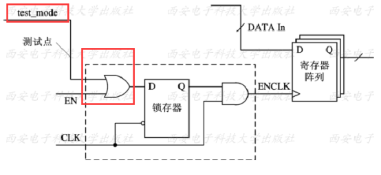
The above diagram shows an example of inserting a control point in the gating logic. In this example, the DFT control signal is “test_mode”, and the control point is located before the latch.
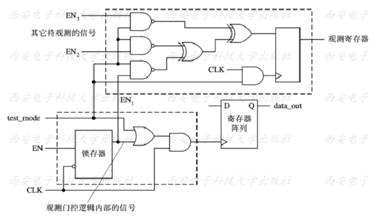
-observation_point option relates to DFT and is used to set whether to insert observation logic to see the internal signals of the gating logic during DFT.
For example, the constraint command below:
set_clock_gating_style -observation_point true
Sets the insertion of observation logic, as shown in the following diagram:
In addition to the options mentioned above, the command has several other options, such as -setup option for setting setup time constraints, -hold option for setting hold time constraints, -observation_logic_depth option for setting the number of XOR gates in the observation circuit, and -max_fanout option for setting the maximum number of loads driven by a gating unit, defining the maximum fanout of the CG unit to reduce clock delays after CG, as the larger the fanout of the gated clock unit, the longer the delay to the registers; additionally, it is used to constrain rebalancing (which will be introduced later). The “set_clock_gating_style” command has many options, and we can use the “man set_clock_gating_style” command in Power Compiler to view its detailed usage.
After setting the style for adding gated clocks, we can set the addition of gated clocks in the gate-level netlist circuit. In Power Compiler, the command insert_clock_gating can be used to add gated clocks to the GTECH netlist. This command can be used alone or with some options to set some functions; we will mainly introduce the -global option below.
Let’s take a look at the following piece of code:
always @ (posedge clk)begin
if (a && b) q=d;
end
When multiple modules have this piece of code, simply using the insert_clock_gating command will yield the following circuit with gated clocks:
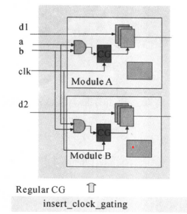
In the above circuit, there are two modules with gated clocks, both controlled by the same control signal. Thus, we can use the insert_clock_gating -global option to allow the gated clock to traverse the hierarchy and insert into the design. This way, it saves both gated clocks and area. Using this option, the synthesized circuit with gated clocks is as follows:
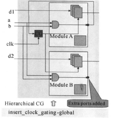
Therefore, using the insert_clock_gating command with the -global option allows the gated clock to traverse the hierarchy. If the -global option is not used, there will be a gated clock unit in each module.
The method of implementing gated clocks is as shown above, mainly involving the two commands of setting the style of gated clocks and adding gated clocks, along with their options.
④ Processing of Gated Clocks
After adding gated clocks to the gate-level netlist, sometimes we need to modify the gated clocks, such as deleting some gated clocks. Below, we will introduce some common processing of gated clocks.
Reconnecting Gated Clocks
As shown in the diagram below:
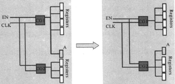
In the left diagram above, register A is triggered by CG1 (originally controlled by the gated unit CG1 above). Since register A is closer to the gating clock unit CG2, we prefer to connect register A to the gating unit CG2 to reduce the wiring length, so we need to reconnect. After reconnection, register A is triggered by CG2, as shown in the right diagram above. The command used for reconnection is as follows:
rewire_clock_gating -gating_cell CG2 -gated_objects {reg_A}
Additionally, we can use the rewire_clock_gating -proximity option; when this option is used, Power Compiler will automatically reconnect registers so that the connection from the clock gating unit CG to the registers is the shortest:
rewire_clock_gating -proximity
Rebalancing the Fanout of Gated Clocks
As shown in the diagram below:
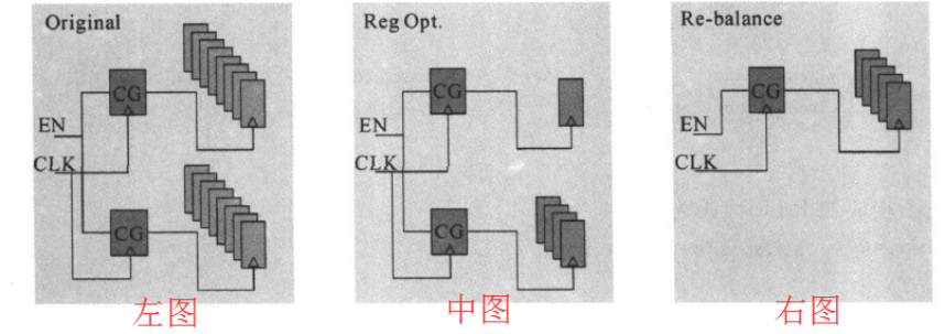
The left diagram shows the original design. When we optimize the circuit (for example, using the compiler_utral -retiming or optimize_registers command), the registers in the design may be moved or deleted, as shown in the middle diagram.
After register optimization, the fanout of the gated clock becomes unbalanced. Since gated clocks have minimum and maximum fanout constraints, the minimum fanout condition cannot be satisfied for each individual CG unit (as shown in the middle diagram). The Power Compiler requires relevant commands to rebalance the fanout of gated clocks, as follows:
rewire_clock_gating -balance_fanout
After executing the above command, the Power Compiler will merge CG units to meet the minimum/maximum fanout constraints. The design after rebalancing is shown in the right diagram.
Merging Gated Clocks
If two or more gated clock units have equal input logic, they can be merged. Merging can only occur within the same hierarchy. After merging, redundant logic is removed. As shown in the diagram below:
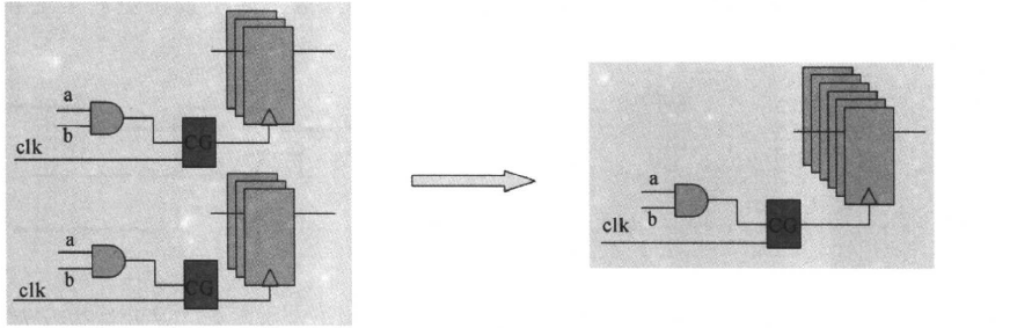
The command for merging is “merge_clock_gating_cells”
Deleting Gated Clocks
Sometimes, we need to delete certain gated clocks; in this case, we can use the remove_clock_gating command. This command has some options as follows:
remove_clock_gating
[-gating_cells CG_cells_list]
[-gated_registers gated_register_list]
[-all] [hier]
As shown in the diagram below:
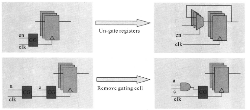
The upper half of the diagram shows the use of the -gated_registers option, which replaces the original gated unit with the “enable-load” mode; the lower half of the diagram shows the use of the -gating_cells option, which deletes the original gated clock.
Therefore, we can delete gated clocks by specifying the gating clock unit or by specifying registers. If the remove clock gating command is used with the switch option “-all”, all gated clocks in the current design will be deleted.
⑤ Manually Inserting Gated Clocks
The above discussion focused on using EDA tools to automatically generate gated clocks with code. We can also manually design gated clocks; below is an example code for manually designing a gated clock:
assign Gated_Clock = Clock&Enable ;
always@(posedge Gated_Clock or negedge Reset)begin
if(!Reset)
Data_ Out<=8’b0;
else
Data Out<=Data Out+8’b1
end
For manually gated clocks, the Power Compiler will not insert clock gating units, nor can it operate on them (such as rebalancing).
Manually gated clocks can be replaced, and the replacement script is as follows:
······
create_clock -period 5 [get_ports clk]
set_clock_gating_style …
replace_clock -gating_cells
······
The circuits before and after replacement are as follows:

The benefits of replacing manually gated clocks include: after replacement, it can avoid potential glitches and also allow the use of other CG commands on it, such as using the remove_clock_gating command to remove the gated clock or using the rewire_clock_gating command to reconnect the gated clock.
The discussion on low-power design with gated clocks ends here; we will not cover the issues related to STA, DFT, and CTS.
(5) Others
Sometimes, we inadvertently introduce unnecessary toggling, which causes additional power consumption. Below is an example of unnecessary toggling (similar to operand isolation):

In the above diagram, when load_out is invalid, if load_op is valid, the data will be operated on, resulting in corresponding toggles. Since the output is invalid, these toggles are unnecessary, consuming power without yielding output. Therefore, we should ensure that when load_out is invalid, load_op is also set to invalid, thereby saving some power consumption.
For the above unnecessary toggling, we can perform appropriate compression to save power, as shown below:

sel_in simultaneously controls the data input and the output of the multiplexer. When SEL=0, A and B are read in, enabling operation 1; when SEL=1, C and D are read in, enabling operation 2; this can reduce the toggling caused by the other half of the operation, thereby reducing power consumption.
For this type of data input followed by selective output operations, gated clocks can be used to reduce unnecessary toggling, thus reducing power consumption.
Combining synthesis for RTL-level low power is as described above, focusing on the use of gated clocks and operand isolation techniques, which are essential for us front-end designers to understand.