Today, I plan to start a new series on low power design. Although my experience in low power design is not extensive, I have worked on projects with high demands for low power consumption, so I have a general understanding of the common practices and main techniques in low power design. Additionally, due to various limitations such as product type, technology, and market conditions, many individuals in certain companies have had no exposure to low power design. Therefore, I would like to take this opportunity to share some of my basic experiences and insights.
That said, I must admit that I am not an expert in low power design, and I may not fully understand many details. I hope that experienced colleagues can discuss and share their knowledge.
Today, I would like to start with the basic concepts. Those who are already familiar with these concepts can skip ahead.
The pursuit of low power design arises from the ever-expanding functionality of chips, increasing operating frequencies, and the resulting high power consumption and heat generation, which increasingly impact the overall performance of devices. The issues of high power consumption and heat generation in CPUs are well-known, which is why many computers require additional cooling devices. In mobile devices, the intervals between charges are becoming shorter, which is partly due to the lack of significant breakthroughs in battery technology, but the high power consumption of chips is also to blame. Therefore, many years ago, the industry began extensive theoretical and practical attempts at low power design, accumulating many effective methods that are still widely used today.
In principle, power consumption refers to power, which is the energy consumed per unit time. We will not elaborate on the principles of power consumption here, but will directly introduce the common low power design approaches used in chip design:
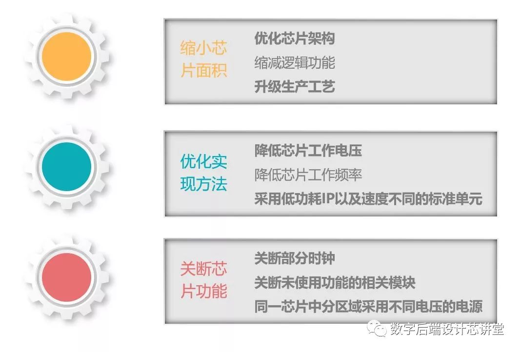
The above lists some common low power design directions in the field of chip design, among which the most frequently applied are optimizing chip architecture, upgrading manufacturing processes, reducing chip operating voltage, using standard cells with different speeds, employing different voltage supplies in different regions, and module shutdown (multi-voltage domains). The following are the main methods related to back-end design:
Upgrading manufacturing processes;
Reducing chip operating voltage;
Shutting down part of the clock (Clock Gating);
Using standard cells with different speeds (Multi-Vth library);
Multi-voltage domain design (Multi-Voltage).
Before explaining the above concepts in detail, I would like to briefly mention the main components of power consumption in chips. Chip power consumption is mainly divided into static power consumption and dynamic power consumption, as illustrated in the following diagram:
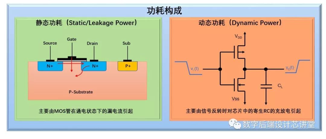
For details on static and dynamic power consumption, please refer to previous articles in this column: How is the overall power consumption of a chip calculated? The various low power design techniques mentioned above aim to reduce these two aspects of power consumption. Below, we will explain in detail several low power design methods closely related to back-end design.
-
Upgrading Processes
This is one of the most widely used and effective methods. The principle is that as transistor sizes decrease, leakage power becomes a larger proportion of overall chip power consumption. Advanced process technologies feature smaller transistor sizes and lower leakage currents, thereby reducing overall leakage power. This is why we often see news reports stating that a certain chip has upgraded from 22nm to 14nm, achieving an x% performance improvement and a y% reduction in power consumption. While the reduction in power consumption may include architectural improvements, the advantages brought by process upgrades are certainly significant.
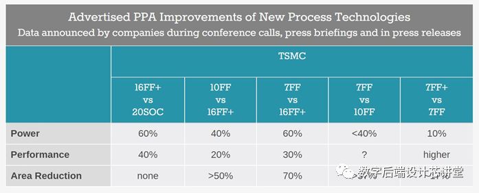
The above image compares the PPA of several recent generations of processes from TSMC’s public data. The trends in process parameters from other foundries should be similar. For this reason, many SoCs used in smartphones, including but not limited to Apple’s A series, Qualcomm Snapdragon series, Huawei Kirin series, and Samsung Exynos series, are eager to adopt the most advanced processes in each generation, as the power and performance advantages of advanced processes are too significant to ignore.
-
Reducing Chip Operating Voltage
According to the physics formula taught in high school, power is directly proportional to the product of voltage and current. Although calculating power consumption on a chip is not that simple, reducing chip voltage remains the most intuitive and effective method for lowering power consumption. Consequently, the operating voltage of most chips has decreased from the initial 5V and 3V to below 1V, and even below 0.5V. However, the challenge is that as voltage decreases, the speed of standard cells also slows down, while electronic devices increasingly demand higher processing speeds, i.e., higher chip frequencies. For example, the initial chip frequencies were only a few hundred megahertz, while the peak frequency of today’s fastest mobile SoCs has exceeded 2GHz. This is one of the technical challenges that must be addressed with each generation of chip upgrades.
-
Shutting Down Clocks (Clock Gating)
Dynamic power consumption is primarily caused by signal transitions, and in chips, the most frequently toggled signal is the clock signal. We know that the transmission of various logic functions and data storage in chips is composed of the following timing paths:
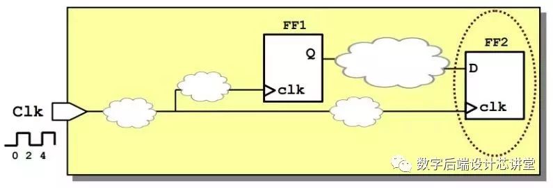
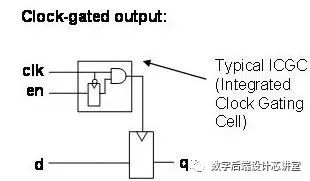
In simple terms, the data from the FF1 register is captured by the FF2 register after a series of operations under the influence of the clock signal clk, completing a data transfer. However, in practice, there may be situations where the data passed from FF1 to FF2 is the same as the data currently stored in FF2, meaning that FF2’s data does not need to be refreshed to maintain functional correctness, yet clk still toggles once to refresh FF2’s data. While this situation poses no functional issues, it represents a real waste of power. Therefore, during the circuit design and logic synthesis phases, designers and EDA tools will insert a series of clock gating cells based on the chip’s functionality and actual data change conditions, ensuring that signals only toggle when data changes. Below is a typical structure of Integrated Clock Gating (ICG):
-
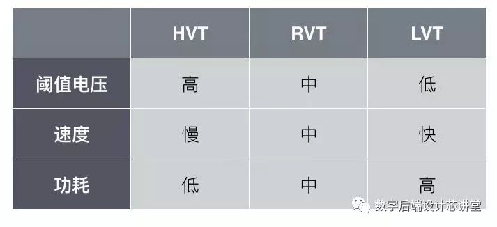
Using Standard Cells with Different Speeds (Multi-Vth Library)
This is one of the most commonly used and easiest design methods in the current chip industry. Vth refers to the threshold voltage of logic gates. The relationship between threshold voltage, power consumption, and speed is as follows: the higher the threshold voltage, the slower the cell speed and the lower the power consumption; conversely, the lower the threshold voltage, the faster the cell speed and the higher the power consumption.
In practical applications, the general strategy is to use cells with lower Vth for modules with high performance requirements or higher frequency parts, allowing setup to converge more easily; for modules with lower performance requirements or lower frequency parts, cells with higher Vth are used to reduce power consumption. This method allows for the adjustment of cell usage on the same chip based on different performance and power consumption requirements, thereby avoiding excessive power consumption on less critical functions.
-
Multi-Voltage Domain Design (Multi-Voltage, Power Gating)
When using a mobile phone, we often encounter situations where, upon seeing the battery is low and lacking a charging device, we try to close all applications, stop listening to music, stop watching videos, and even turn off location and navigation functions. The fundamental purpose is to reduce the functions that consume battery power. This concept has also been introduced into chip design: an SoC may contain many functional modules such as video processing (DSP), audio processing (AUDIO), positioning (GPS), gaming (GPU), memory (Memory), etc., but most functions do not operate simultaneously. Therefore, to reduce the power consumption of unused modules in a waiting state, they are designed to be turned off when not in use. This is the initial idea behind Power Gating. At the same time, for high-performance modules like CPUs and GPUs, which require higher frequencies, higher voltages may be used in design, while less critical modules like AUDIO and GPS can be designed with relatively lower voltages. As a result, the entire chip may look like the following (the image does not represent any actual chip):
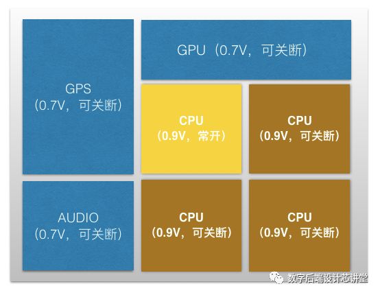
In this way, the chip’s power consumption can be minimized, with only one CPU core active, significantly reducing the power consumption of other modules while waiting, thus extending battery life.
Although the concept is simple, in actual design, both different voltages and module shutdown can introduce many additional issues. We will discuss these problems and the commonly used solutions in the industry in future articles.
This concludes the introduction to the basic concepts of low power design. This article assumes that readers have a basic understanding of chip design concepts. If anyone has any unclear concepts or terms, please leave a message or join the discussion group.
Recommended previous articles:
Back-end Design Challenges in 7nm Process
Fundamentals of Digital Back-end: Detailed Explanation of Noise
Fundamentals of Back-end Concepts: Comprehensive Overview of Various OCV (Part 2)!
Fundamentals of Back-end Concepts: Comprehensive Overview of Various OCV (Part 1)!
Fundamentals of Digital Back-end Skills: Clock Tree Synthesis (CTS) Part 2
New Concepts in Digital Back-end: What is Inbound Cell?
SNUG 2018 Highlights: Machine Learning Has Finally Arrived!
Fundamentals of Digital Back-end Skills: Clock Tree Synthesis (CTS) Part 1
Fundamentals of Digital Back-end Skills: How to Resolve Routing Congestion?
A Guide for Chip Design Beginners: What is the Basic Process of Back-end Design?
Fundamentals of Digital Back-end: How is the Overall Power Consumption of a Chip Calculated?
Fundamentals of Back-end Timing: Why is ICG Prone to Setup Violations?
Fundamentals of Back-end Timing: Why Must Sequential Circuits Meet Setup and Hold Times?
Fundamentals of Back-end Timing Skills: How to Fix Hold Violations?
Fundamentals of Back-end Timing Skills: How to Fix Setup Violations?
If anyone has any questions about back-end technology and career development, or if there are any technical topics related to digital back-end that you would like to learn about and discuss, feel free to scan the QR code on the left to join the digital back-end discussion group.
To avoid spreading advertisements, please also send verification information answering the following question:
Who are the mainstream EDA tool vendors in IC design besides Synopsys and Mentor (Siemens)?
Also, feel free to scan the QR code on the right to follow my Zhihu:
Zhihu Account: Yan Futi
Zhihu Column: The Path of Digital IC Back-end Design Engineer.