1. The Endless Demand for Chip Miniaturization
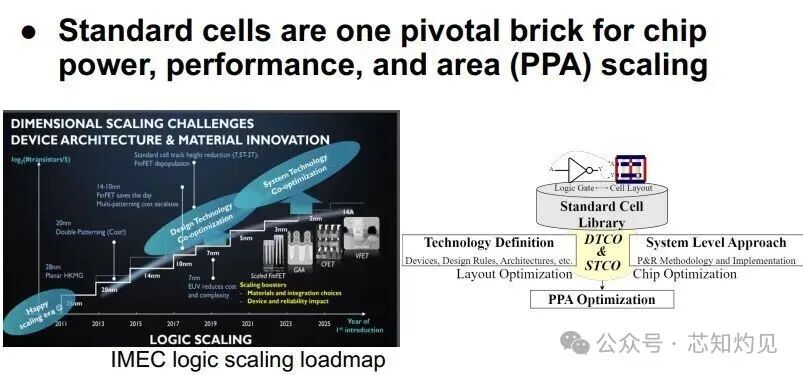
2. Standard Cell Layout
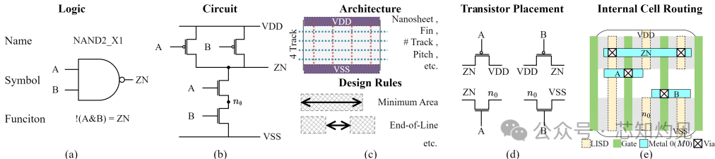
The standard cell layout generation process consists of five core steps
-
Logic Definition (e.g., NAND2_X1 functional symbol)
-
Circuit Implementation (PMOS/NMOS transistor network)
-
Architectural Parameters (device selection/number of tracks/metal spacing)
-
Transistor Layout (gate alignment/diffusion sharing)
-
Internal Wiring (meeting design rules and pin accessibility)
3. Three Major Technical Challenges
3.1 Transistor Partitioning
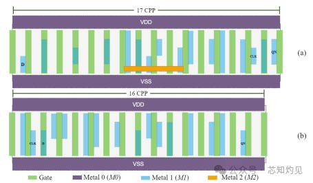
Heuristic Partitioning: Quickly groups based on design hierarchy, but leads to area loss (DFFHQN_X1 width increases by 1 CPP)
Exhaustive Search: Achieves optimal layout (width reduced by 1 CPP), but computational complexity grows exponentially
3.2 Gear Ratio & Offset
Resource Conflict: CPP stagnates at 42nm, while metal spacing continues to shrink to 22nm
2:3 GR Cost: Non-uniform grid requires an additional 1/3 offset to achieve a legal layout
Innovative Solution: 1:1 (+½) offset releases M1 layer resources, avoiding CPP increase
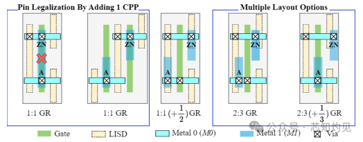
Gear Ratio: The ratio of Contacted Poly Pitch (CPP) to M1 Pitch
Offset: The distance from the cell origin to the leftmost M1 column
1:1 GR: Uniform grid, all vertical columns (polysilicon/M1) aligned, but can lead to tight wiring resources.
2:3 GR: Non-uniform grid, requires additional offset (e.g., \frac{1}{3} CPP) to release wiring resources (Figure 4c).
3.3 PPA Metric Trade-offs
Compact Layout (5 CPP) ⇒ 30% area savings, but pin access points reduced to 7
Loose Layout (6 CPP) ⇒ Area loss, but pin access points increase to 10, improving routability
4 Future Directions
4.1 Logic Optimization
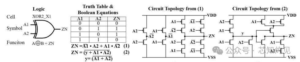
XOR2 cell Boolean restructuring: Sum of products form (12 transistors) → Hierarchical structure (10 transistors)
4.2 Topology Optimization
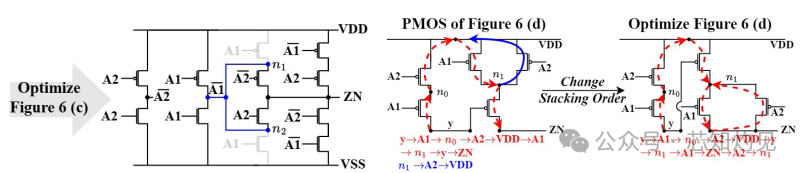
Euler Path Optimization: Adjusting PMOS stacking order to achieve diffusion area sharing (saves 1 CPP)
Drive Enhancement Scheme: X2 transistors split into dual X1 structure, reducing RC delay by 40%
4.3 Standard Cell Merging Technology
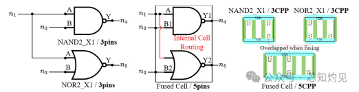
NAND2+NOR2 merging scheme: Sharing input pins, reducing total pin count from 6 to 5, compressing layout width by 1 CPP, breaking the “pin density wall”
4.4 New Device Integration
| Device Type | Advantages | Technical Challenges |
| MESO Devices | Operates at 100mV ultra-low voltage | Magnetoelectric-spin-orbit 3D interconnect architecture |
| TFT Devices | Low-temperature process compatible with 3D-IC | No P-channel asymmetric design |

Reference:
Chung-Kuan Cheng, Byeonggon Kang, Bill Lin, and Yucheng Wang. 2025. Standard Cell Layout Generation: Review, Challenges, and Future Works. Proceedings of the 30th Asia and South Pacific Design Automation Conference. Association for Computing Machinery, New York, NY, USA, 372–378.