Standard Cell Layout Generation: Review, Challenges, and Future Work
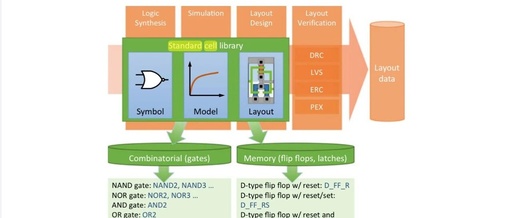
1. The Endless Demand for Chip Miniaturization 2. Standard Cell Layout The standard cell layout generation process consists of five core steps Logic Definition (e.g., NAND2_X1 functional symbol) Circuit Implementation (PMOS/NMOS transistor network) Architectural Parameters (device selection/number of tracks/metal spacing) Transistor Layout (gate alignment/diffusion sharing) Internal Wiring (meeting design rules and pin accessibility) 3. Three … Read more