1. Overview
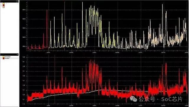
Managing chip voltage drop is crucial for ensuring the stable operation of integrated circuits (IC), involving multiple levels such as the printed circuit board (PCB), packaging, and within the chip itself. Specific recommended metrics vary based on application domain, process node, chip type, etc., but here are some general guidelines and reference metrics:
-
1. PCB Level
•Resistance of power and ground layers: The target is typically less than 1mΩ/square (square inch), with specific values depending on current density and application requirements.
•Decoupling capacitor layout: It is generally recommended to configure at least 10uF of decoupling capacitance per 1 square inch of logic area, and additional ceramic capacitors (such as 0.1uF or 1nF) should be added for high-frequency applications to handle high-frequency transient currents.
•Voltage fluctuation: The target for dynamic voltage fluctuation (ΔV) should be less than 5% of the supply voltage; for example, under a 3.3V supply, ΔV should be less than 0.165V.
-
2. Package Level
•Package pin resistance: The resistance (or impedance) of package pins should be controlled within a few milliohms (mΩ), with specific values depending on package type and design requirements.
•Package inductance: The inductance within the package and from the package to the PCB should be kept as low as possible; ideally, the inductance within the package should be less than 1nH to reduce voltage spikes at high frequencies.
•Thermal resistance: The thermal resistance of the package (θjc) affects the chip’s heat dissipation; for high-performance applications, thermal resistance should be less than 10°C/W.
-
3. Chip Internal
•Power grid resistance: The resistance of the internal power grid of the chip should be maintained at the nanohm level (nΩ) to ensure that the voltage drop across the entire chip remains minimal.
•Maximum allowable voltage drop: It is generally considered that the maximum allowable voltage drop within the chip should not exceed 5% of the supply voltage, and it is recommended to control it within 3% to ensure that the threshold voltage of logic gates is not affected, maintaining stable circuit operation.
•Electromigration limits: To prevent electromigration, the local current density should generally not exceed a few million amperes per square centimeter (A/cm²), with specific values depending on process nodes and material properties.
Comprehensive Strategy
•Simulation verification: During the design process, use simulation software such as Sigrity and Ansys to perform IR Drop simulations across the entire link, ensuring that the above metrics are met even under worst-case scenarios.
•Dynamic testing: After the design is completed, conduct dynamic testing on the actual product to verify voltage stability under various operating conditions, ensuring that the design meets expectations.
Please note that these data are based on general recommendations, and specific projects should be evaluated and adjusted based on actual design requirements, process capabilities, and performance goals.
2. Die IR Drop Analysis
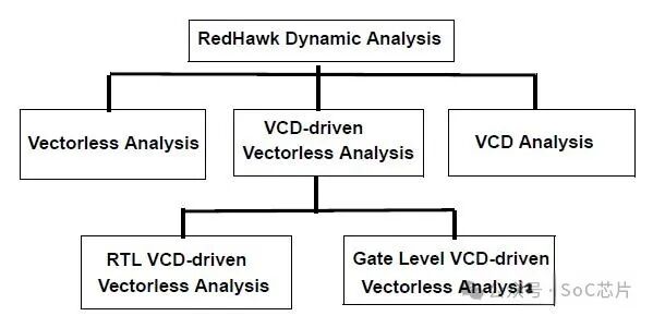
The IR drop analysis within the chip die is a critical aspect of semiconductor design, directly related to the chip’s performance and reliability. Inside integrated circuits (IC), as current flows through the power network (power grid), the product of the network’s resistance (R) and current (I) causes a voltage drop. Here are several key steps and considerations for IR drop analysis within the chip die:
-
1. Model Establishment
•Physical model construction: First, a physical model of the chip die needs to be established, including the layout and dimensions of power lines, ground lines, transistors, capacitors, and their electrical connections.
•Resistance network model: Simplify the power network into a resistance network model by calculating the resistance values of different metal layers, vias, and interconnections to assess the overall resistance distribution of the network.
-
2. Current Distribution Analysis
•Static current analysis: Calculate the static current distribution of the chip when inactive, typically based on the static power consumption of the design.
•Dynamic current analysis: Use simulation tools (such as SPICE) to simulate the dynamic current behavior of the chip under different operating states, considering factors like signal transitions and clock activity that affect current distribution.
-
3. Voltage Drop Simulation
•Static IR drop simulation: Calculate the voltage drop across the power network based on the static current distribution, assessing voltage stability without timing constraints.
•Dynamic IR drop simulation: Consider the impact of instantaneous current changes on voltage, simulating voltage fluctuations under various operating modes, especially under high load conditions.
-
4. Critical Area Identification
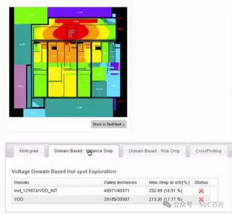
•Hotspot analysis: Identify areas with the highest voltage drop through simulation results, typically where current density is high or the power network resistance is significant.
•Timing analysis: Evaluate the impact of voltage drop on circuit timing paths, including setup and hold times, ensuring timing convergence.
-
5. Optimization Strategies
•Power grid improvement: Optimize the layout of power and ground networks, increase metal layers, and use larger cross-sectional metal lines to reduce resistance.
•Decoupling capacitor optimization: Layout decoupling capacitors in critical areas to absorb instantaneous current spikes and reduce voltage fluctuations.
•Current balancing: Adjust circuit design to balance current distribution as much as possible, avoiding local overheating and voltage drops.
-
6. Verification and Sign-off
•IR drop sign-off: Ensure that under all expected operating conditions, the voltage drop meets design specifications and does not lead to functional errors in the circuit.
•EMC/Thermal analysis: Simultaneously consider electromagnetic compatibility and thermal management to ensure chip stability and reliability under high power operation.
-
7. Iterative Optimization
•Design iteration: Based on simulation and analysis results, adjust the design and re-simulate until all metrics meet requirements.
In summary, IR drop analysis within the chip die is an iterative and complex process that requires comprehensive consideration of design, simulation, optimization, and verification aspects to ensure that the chip can operate stably and efficiently in practical applications. With advancements in semiconductor processes and increasing design complexity, this process has become increasingly important and is a key step in enhancing chip performance and reducing power consumption.
3. Package IR Drop Analysis
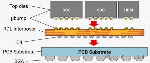
The IR drop analysis in chip packaging is a complex and important process that involves evaluating voltage loss within the package to ensure that the chip can operate normally after packaging without being affected by power fluctuations. Package-level IR drop analysis primarily focuses on the voltage loss along the power transmission path from the external power source to the chip’s interior. Here are the key steps and considerations for conducting package IR drop analysis:
-
1. Package Model Construction
•Physical model: First, an accurate package model needs to be constructed, including package materials (such as substrates, lead frames), the resistance and inductance values of power and ground lines within the package, and solder joints (such as bumps under Flip Chip or wires in Wire Bond).
•Electrical model: Use three-dimensional electromagnetic simulation software (such as ANSYS HFSS, Cadence Sigrity, etc.) to establish the electrical model of the package, simulating current flow and electric field distribution at different frequencies.
-
2. Current Distribution Analysis
•Extract current waveforms: Based on the chip’s power distribution and operating modes, extract current waveforms under different conditions, including peak current, average current, and transient current variations.
•Current paths within the package: Analyze how current flows through various parts of the package, including pins, substrates, and internal interconnections, to identify potential high-resistance or high-inductance areas.
-
3. IR drop Simulation
•Static analysis: Perform static IR drop simulation to assess voltage drop under fixed current conditions, ensuring uniform voltage distribution across the entire package.
•Dynamic analysis: Execute dynamic simulations considering transient current effects, evaluating the extent of voltage fluctuations during switching operations and high-load conditions, which is particularly important for high-speed signals and sensitive circuits.
-
4. Thermal Effects Consideration
•Thermal analysis: The temperature rise of the package can lead to increased resistance, thereby affecting IR drop. Therefore, conduct thermal analysis to incorporate temperature effects into IR drop simulations, ensuring the accuracy of analysis results.
-
5. Optimization and Improvement
•Design optimization: Based on simulation results, optimize package design, such as increasing or optimizing decoupling capacitor layout, improving power and ground line structures, and selecting low-resistance materials to reduce IR drop.
•Power distribution strategy: Consider using multiple power pins and optimizing the power distribution network (PDN) design to ensure stable power supply.
-
6. Verification and Sign-off
•Sign-off standards: Set allowable ranges for IR drop based on industry standards and specific application requirements, ensuring the chip’s performance and reliability after packaging.
•Post-packaging testing: Conduct tests on actual packaged samples to verify simulation results and make adjustments if necessary.
-
7. System-Level Considerations
•Cooperative optimization with PCB: The IR drop analysis of the package cannot be conducted in isolation; it needs to be considered in conjunction with the PCB power distribution network design to ensure power integrity at the system level.
Through the above steps, effective analysis and management of IR drop in chip packaging can be achieved, ensuring the chip’s performance after packaging and reducing functional failures and reliability issues caused by power fluctuations.
4. PCB Board IR Drop Analysis
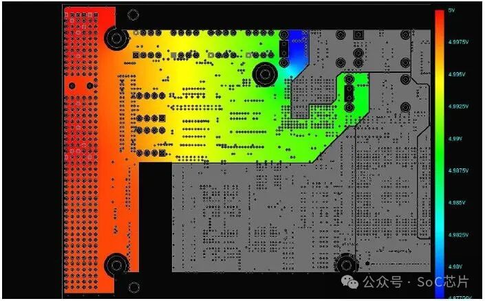
The IR drop analysis on the PCB (Printed Circuit Board) is a key step in ensuring the stable operation of electronic devices, assessing the voltage loss caused by resistance effects as current flows through the PCB power network. Here are the main steps and considerations for conducting IR drop analysis on the PCB board:
-
1. Modeling and Preparation
•Power network modeling: Use EDA (Electronic Design Automation) tools such as Cadence Allegro, Mentor Graphics HyperLynx, or Altium Designer to establish the power network model of the PCB. This includes power planes, ground planes, power traces, decoupling capacitors, and the traces connecting these components.
•Current demand analysis: Estimate the current consumption of various parts under different operating modes based on the circuit design. This may involve static current analysis (DC) and dynamic current analysis (AC), considering clock speeds, signal transition rates, and other factors.
-
2. Simulation Setup
•Set simulation parameters: Input power voltage, current waveforms, ambient temperature, and other parameters into the simulation software to ensure that the simulation conditions closely match the actual operating environment.
•Determine simulation scope: Select the simulation time window and frequency range of interest to capture both transient and steady-state behavior.
-
3. IR drop Simulation
•Static IR drop analysis: Calculate the voltage drop across the power network under static conditions without signal changes, ensuring voltage stability under static conditions.
•Dynamic IR drop analysis: Simulate transient current changes in the circuit under different operating modes, assessing voltage fluctuations, especially for high-speed signals and high-power components.
-
4. Result Analysis
•Hotspot identification: Analyze simulation results to identify areas with the highest voltage drop, typically where current density is high or resistance is significant.
•Timing analysis: Evaluate the impact of voltage drop on signal integrity, including whether it leads to timing violations (such as setup and hold times).
-
5. Optimization and Adjustment
•Power plane optimization: Reduce the total resistance of the power network by increasing the copper thickness of the power plane, optimizing plane layout, and minimizing segmentation.
•Decoupling capacitor optimization: Properly layout decoupling capacitors, especially near high-power components, to quickly respond to transient current demands and reduce voltage fluctuations.
•Trace and via optimization: Optimize the width and length of power and signal traces, reducing the number of vias to lower resistance and inductance.
-
6. Verification and Iteration
•Design iteration: Make necessary modifications to the PCB design based on simulation and analysis results, then repeat the simulation and analysis process until all critical areas’ IR drop meets design specifications.
•Physical testing: In the final design stage, actual testing may also be required to ensure that simulation results align with real-world conditions.
Through the above steps, effective management and reduction of IR drop on the PCB board can be achieved, improving the stability and reliability of electronic products and ensuring their performance under various operating conditions.