A good amplifier circuit aims for a high, distortion-free voltage gain (Au) and a high input resistance (Ri), while the output resistance (Ro) should be as low as possible, and the bandwidth should be as wide as possible. The circuits introduced earlier are all BJT common emitter amplifier circuits, which can achieve a relatively high voltage gain (Au) ranging from tens to hundreds, effectively amplifying small signals without distortion. However, the input resistance (Ri) is not sufficiently high, and the output resistance is not low enough. If a high input resistance and a low output resistance are desired, a common collector amplifier circuit structure can be used.
In the Multisim workspace, the common collector amplifier circuit is built as shown in the figure below. V2 is in series with R2 to form the input signal; R4 serves as the load, and the voltage across it is the output voltage. It can be seen that the BJT collector is connected to the positive terminal of the DC power supply V1. When drawing the AC path, the DC power supply V1 can be considered a short circuit, meaning that in the AC path, the BJT collector is directly grounded, serving as the common terminal for the input small signal and the output signal, hence it is called a common collector circuit. Additionally, since the load R4 is connected to the BJT emitter through a capacitor C2, it is also referred to as an emitter follower.
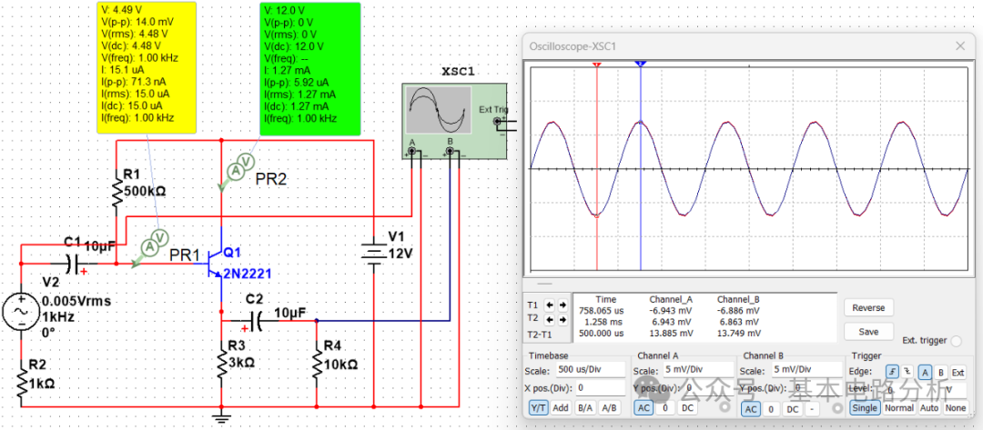
(1) Start the simulation, and the probe PR1 indicates that the BJT base DC potential is 4.48V, and the base DC current is 15.0uA. The probe PR2 indicates that the collector DC potential is 12V, and the collector DC current is 1.27mA, confirming that the BJT is in the amplification state. The theoretical derivation shows that the AC voltage gain of this circuit isAu=(1+β)(R3//R4)/[rbe+(1+β)(R3//R4)]≈0.99. From the oscilloscope waveform, it can be seen that the output voltage closely matches the input voltage signal. At time T1, the input signal is -6.943mV, and the output signal is -6.886mV, thusAu=-6.886/-6.943≈0.99, which is consistent with the theoretical derivation. This indicates that the common collector amplifier circuit has a voltage gain less than 1, but approximately equal to 1.
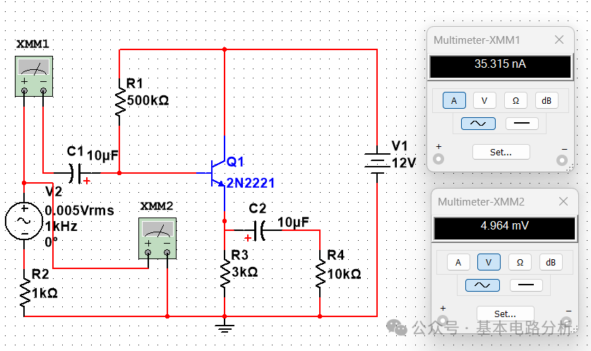
(2) Remove the probes and oscilloscope, insert the multimeter XMM1 in series with V2 branch to measure the AC current at the input port. Use XMM2 across V2 and R2 to measure the AC voltage at the input port. The simulation results are shown in the figure below. The input resistance Ri=4.964/0.035315≈141kΩ (quite large). Readers can derive the input resistance of this circuit and compare it with the measured results.
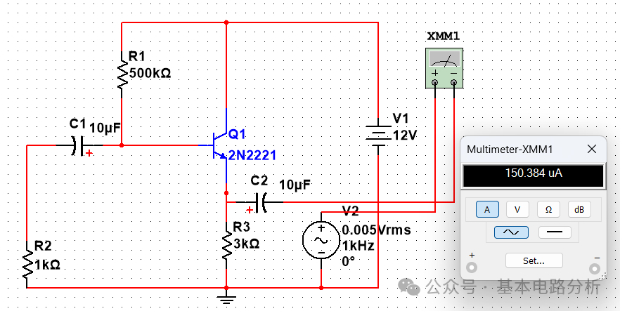
(3) Short-circuit the input port V2 and open the load R4. Then move V2 to the original position of R4. Use the multimeter XMM1 to measure the AC current in the V2 branch. The simulation results are shown in the figure below. The output resistance Ro=5/0.150384≈33Ω (very small). Readers can also derive the output resistance of this circuit and compare it with the measured results.
As mentioned earlier, although the voltage gain of the common collector amplifier circuit is less than 1, it has the advantages of high input resistance and low output resistance. Due to the high input resistance, it is often used as the first stage in multi-stage amplifier circuits to increase input resistance and reduce the burden on the signal source. Because of the low output resistance, it is commonly used as the last stage in multi-stage amplifier circuits to lower output resistance and improve load-driving capability. Utilizing the characteristics of high input resistance, low output resistance, and Au ≈ 1, the emitter follower can also be placed between two stages of an amplifier circuit to serve as an impedance matching stage, at which point the emitter follower is referred to as a buffer stage or intermediate isolation stage.